Tool/software:
Question1:
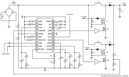
In the datasheet, it is suggested to use a current transformer in series with the power switch to detect the current, then synthesize the inductor current waveform inside the IC.
But in this way, the commutation loop will be expanded to increase the loop impedance. And I am afraid that the switching node is noisy. May I check if the following options are feasible? And which one would you recommend?
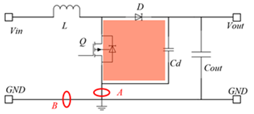
- Put the CT on the GND side, point A, which is out of the commutation loop.
- Put the CT in series with the GND trace, point B, to detect the inductor current directly.
- Put a shunt resistor instead of a CT on point A or point B. If so, how to select the external components, i.e., RSYN
Question2:
And in the schematic, I found some ferrite beads in series with the MOSFETs and diodes. May I ask why you are placing them? What are the problems you want to solve? How to select these ferrite beads? 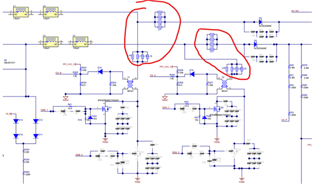
Especially, the turn-on/turn-off transient of these power switches is very quick. di/dt is quite high. Will that cause high voltage spikes across the devices?
Question3
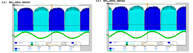
Looked into the details of the test report do find some big voltage spikes across the MOSFETs. Apparently, when the current is higher, di/di is higher (assuming rising time and falling time remain the same), and voltage spikes are higher. The output voltage is 390V, but the maximum Vds is 498V. I think it is very likely caused by the ferrite beads in series with power switches. Did TI have any other concerns placing the ferrite beads there?