Part Number: TPSM64406
Tool/software:
Background:
I've downloaded the TPSM6440x Quickstart Tool REVB to my computer and unblocked it in the Windows Properties dialog.
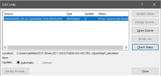
Question 1: The following look like leftovers and a broken link from copy-paste errors. What functionality is the spreadsheet missing?
When opening the tool in Excel and enabling active content (bar at top), I get the following notice:

When I click on either "Continue" or "Edit Links..." I get:

When I open the highlighted link source, I get:

A path on a TI computer or server perhaps?
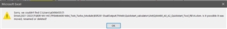
Question 2 - The RESET VALUES button in "Step 9: External Loop Compensation Design" raises the following error dialogs. I assume the button is intended to be a macro to reset the compensation component values to the recommended ones. Is that the only functionality that's missing?:
Pressing the RESET VALUES button raises the following:

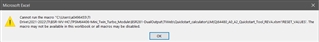
Clicking OK raises the following:

Question 3 - In "Step 3: Internal Buck Inductor" the DCR of the module's buck inductor is 68mΩ @25°C. What is the source of that value? I cannot find it in the data sheet.
Question 4 - Since the inductor is fixed, is Step 3 only useful for choosing switching frequency? A couple of notes in Step 3 as well as recommended "Inductance for 35% Ripple Current..." make this section seem like a copy-paste from another calculator.
Question 5 - When performing a dual-output design, the module's loop compensation is internal (Step 8 compensation fields not available). In Step 6, "Output Capacitors", Undershoot Transient and Crossover Frequency fields appear to do nothing, should they also be made unavailable?
Question 6 - In In Dual Output mode, "Step 6, Output Capacitors", changing Cout and its ESR make changes to the Loop Response plot and, consequently, phase and gain margins. Despite the apparently non-functional fields (in Question 5), is the Loop Response plot still valid?