This thread has been locked.

If you have a related question, please click the "Ask a related question" button in the top right corner. The newly created question will be automatically linked to this question.

AFE7950EVM: Serdes FIFO error in AFE750+TRF1208 EVM module

Part Number: AFE7950EVM
Other Parts Discussed in Thread: AFE7960, TRF1208, AFE7950

Tool/software:

Dear Team, 

I am trying to take the DAC output from AFE7960+TRF1208 EVM used along with TSW1457EVM.

I have given LMK clock as 3GHz at 10 dBm and the AFE reference clock as 12 GHz at 10 dBm according to our requirement. The input voltage given for the EVM module is 5.5V@4A and for the FPGA board TSW14J57 is 12V@4A .

But while running the script in latte, the following attached error is observed.

I tried the method of clicking “Send” for the DAC pattern multiple times in HSDC and running the command “AFE.adcDacSync(1)”. But the same error was observed

Please suggest a solution for this.

  • Dear team,

    The EVM module part number is AFE7950+TRF1208 EVM.

    Regards,

    Mithuna Krishnakumar

  • Kindly find the log window for the above mentioned error.

    #======

    #Executing .. AFE7950/bringup/setup.py

    #Start Time 2025-03-07 09:11:58.332000

    AFE79xxLibraryPG1p0

    spi - USB Instrument created.

    resetDevice

    Kintex RegProgrammer - USB Instrument created.

    Kintex RegProgrammer - USB Instrument created.

    Kintex RegProgrammer - USB Instrument created.

    #Done executing .. AFE7950/bringup/setup.py

    #End Time 2025-03-07 09:12:05.142000

    #Execution Time = 6.80999994278 s

    #================ ERRORS:0, WARNINGS:0 ================#

    #======

    #Executing .. AFE7950/bringup/devInit.py

    #Start Time 2025-03-07 09:12:07.932000

    Power Card - USB Instrument created.

    Reset the FPGA and try again.

    Loaded Libraries

    Refreshed GUI

    #Done executing .. AFE7950/bringup/devInit.py

    #End Time 2025-03-07 09:14:04.404000

    #Execution Time = 116.472000122 s

    #================ ERRORS:1, WARNINGS:0 ================#

    #======

    #Executing .. AFE7950/bringup/script18_DAC-ADC-12G.py

    #Start Time 2025-03-07 09:14:17.776000

    For these rates, 1KHz raster mode is not supported. Changing to 32-bit NCO mode.

    The External Sysref Frequency should be an integer factor of: 5.208333MHz

    2T2R1F Number: 0

    Valid Configuration: True

    laneRateRx: 10000.0

    laneRateFb: 10000.0

    laneRateTx: 10000.0

    2T2R1F Number: 1

    Valid Configuration: True

    laneRateRx: 10000.0

    laneRateFb: 10000.0

    laneRateTx: 10000.0

    LMK Clock Divider - Device registers reset.

    LMK Clock Divider - Device registers reset.

    LMK and FPGA Configured.

    DONOT_OPEN_Atharv_FULL - Device registers reset.

    chipType: 0xa

    chipId: 0x78

    chipVersion: 0x11

    AFE Reset Done

    Fuse farm load autoload done successful

    No autload error

    Fuse farm load autoload done successful

    No autload error

    AFE MCU Wake up done and patch loaded.

    AFE PLL Configured.

    AFE SerDes Configured.

    AFE Digital Chains configured.

    AFE TX Analog configured.

    AFE RX Analog configured.

    AFE FB Analog configured.

    AFE JESD configured.

    AFE AGC configured.

    AFE GPIO configured.

    Sysref Read as expected

    ###########Device DAC JESD-RX 0 Link Status###########

    Comma Align Lock Lane0: False; Please check if the transmitter is sending data and eye is good.

    Comma Align Lock Lane1: False; Please check if the transmitter is sending data and eye is good.

    Comma Align Lock Lane2: False; Please check if the transmitter is sending data and eye is good.

    Comma Align Lock Lane3: False; Please check if the transmitter is sending data and eye is good.

    CS State TX0: 0b00000000 . It is expected to be 0b10101010

    FS State TX0: 0b00000000 . It is expected to be 0b01010101

    Couldn't get the link up for device RX: 0; Alarms: 0x0

    ###################################

    ###########Device DAC JESD-RX 1 Link Status###########

    Comma Align Lock Lane0: False; Please check if the transmitter is sending data and eye is good.

    Comma Align Lock Lane1: False; Please check if the transmitter is sending data and eye is good.

    Comma Align Lock Lane2: False; Please check if the transmitter is sending data and eye is good.

    Comma Align Lock Lane3: False; Please check if the transmitter is sending data and eye is good.

    CS State TX0: 0b00000000 . It is expected to be 0b10101010

    FS State TX0: 0b00000000 . It is expected to be 0b01010101

    Couldn't get the link up for device RX: 1; Alarms: 0x0

    ###################################

    AFE Configuration Complete

    #Done executing .. AFE7950/bringup/script18_DAC-ADC-12G.py

    #End Time 2025-03-07 09:15:21.284000

    #Execution Time = 63.507999897 s

    #================ ERRORS:10, WARNINGS:1 ================#

  • Hi Mithuna,

    On the TSW14J57 there is a bank of status LEDs, D1-D9. Can you share the state of these LEDs? 


    Also, can you share the script you are testing? 


    Regards,

    David Chaparro

  • Dear David,

    The above mentioned error has been resolved.

    I just need to clarify the following queries.

    1) Kindly share the details of calibration method of ADC channels.

    2)Can you please suggest the script lines that must be added in order to configure the output power of the DAC channels.

    I have attached the script for your reference.

    ##############        Read me            ##############
    #In HSDC Pro DAC tab, Select AFE79xx_2x2TX_44210; Data Rate = 491.52M
    #In HSDC Pro ADC tab, Select AFE79xx_2x2RX_24410; Data Rate = 245.76M ---> To capture 4 RX channels
    #In HSDC Pro ADC tab, Select AFE79xx_1x2FB_44210; Data Rate = 491.52M ---> To capture 2 FB channels

    sysParams=AFE.systemParams
    sysParams.__init__();sysParams.chipVersion=chipVersion

    setupParams.skipFpga = 1 # setup FPGA (TSW14J56) using HSDC Pro

    ##############        Top Level            ##############
    sysParams.FRef            = 12000
    sysParams.FadcRx        = 3000
    sysParams.FadcFb        = 3000
    sysParams.Fdac            = 12000
    sysParams.externalClockRx=True
    sysParams.externalClockTx=True
    sysParams.RRFMode = 5    
                                        
    ##############        Digital Chain        ##############

            #####    RX    #####       
    sysParams.rxEnable        =    [False,False,False,False]
    sysParams.ddcFactorRx    =    [6,6,6,6]            #DDC decimation factor for RX A, B, C and D
    sysParams.rxNco0        =     [[2200,2200],            #Band0, Band1 for RXA
                                [2200,2200],            #Band0, Band1 for RXB
                                [2200,2200],            #Band0, Band1 for RXC
                                [2200,2200]]            #Band0, Band1 for RXD

            #####    FB    #####

    sysParams.fbEnable        =    [False,False,False,False]
    sysParams.ddcFactorFb    =    [6,6]                    #DDC decimation factor for FB 1 and 2
    sysParams.fbNco0        =     [9500,9500]                #Band0 for FB1 and FB2
            #####    TX    #####
    sysParams.txEnable        =    [True,True,True,True]
    sysParams.ducFactorTx    =    [24,24,24,24]            #DUC interpolation factor for TX A, B, C and D
    sysParams.txNco0        =     [[6000,6000],            #Band0, Band1 for TXA
                                [8200,8200],            #Band0, Band1 for TXB  
                                [6000,6000],            #Band0, Band1 for TXC
                                [8200,8200]]            #Band0, Band1 for TXD
    ##############        JESD        ##############

            #####    ADC-JESD    #####
    sysParams.jesdSystemMode= [3,3]
                                                        #SystemMode 0:    2R1F-FDD                        ; rx1-rx2-fb -fb
                                                        #SystemMode 1:    1R1F-FDD                        ; rx -rx -fb -fb
                                                        #SystemMode 2:    2R-FDD                            ; rx1-rx1-rx2-rx2
                                
                                                        #SystemMode 3:    1R                                ; rx -rx -rx -rx
                                                        #SystemMode 4:    1F                                ; fb -fb- fb -fb
                                                        #SystemMode 5:    1R1F-TDD                        ; rx/fb-rx/fb-rx/fb-rx/fb
                                                        
    sysParams.jesdTxProtocol= [0,0]                        # 0 - 8b/10b encoding; 2 - 64b/66b encoding
    sysParams.LMFSHdRx        = ["44210","44210","44210","44210"]
                                                        # The 2nd and 4th are valid only for jesdSystemMode values in (0,2).
                                                        # For other modes, select 4 converter modes for 1st and 3rd.
    sysParams.LMFSHdFb        = ["44210","44210"]

    sysParams.rxJesdTxScr    = [True,True,True,True]
    sysParams.fbJesdTxScr    = [True,True]

    sysParams.rxJesdTxK        = [16,16,16,16]
    sysParams.fbJesdTxK        = [16,16]

    sysParams.jesdTxLaneMux    = [0,1,2,3,4,5,6,7]            # Enter which lanes you want in each location.
                                                        # For example, if you want to exchange the first two lines of each 2T,
                                                        #        this should be [[1,0,2,3],[5,4,6,7]]

            #####    DAC-JESD    #####
    sysParams.jesdRxProtocol= [0,0]
    sysParams.LMFSHdTx        = ["44210","44210","44210","44210"]
    sysParams.jesdRxLaneMux    = [0,1,2,3,4,5,6,7]            # Enter which lanes you want in each location.
                                                        # For example, if you want to exchange the first two lines of each 2R
                                                        #        this should be [[1,0,2,3],[5,4,6,7]]
    sysParams.jesdRxRbd        = [4, 4]
    sysParams.jesdRxScr        = [True,True,True,True]
    sysParams.jesdRxK        = [16,16,16,16]

            #####    JESD Common    #####
        
    sysParams.jesdABLvdsSync= True
    sysParams.jesdCDLvdsSync= True
    sysParams.syncLoopBack    = True    #JESD Sync signal is connected to FPGA

    ##############        GPIO        ##############
    sysParams.gpioMapping    = {
                            'H8': 'ADC_SYNC0',
                            'H7': 'ADC_SYNC1',
                            'N8': 'ADC_SYNC2',
                            'N7': 'ADC_SYNC3',
                            'H9': 'DAC_SYNC0',
                            'G9': 'DAC_SYNC1',
                            'N9': 'DAC_SYNC2',
                            'P9': 'DAC_SYNC3',
                            'P14': 'GLOBAL_PDN',
                            'K14': 'FBABTDD',
                            'R6': 'FBCDTDD',
                            'H15': ['TXATDD','TXBTDD'],
                            'V5': ['TXCTDD','TXDTDD'],
                            'E7': ['RXATDD','RXBTDD'],
                            'R15': ['RXCTDD','RXDTDD']}

    # device.TOP.IO_WRAP.IO_WRAP.CFG_GPIO.pull_ctrl_gpio_34=3
    # device.TOP.IO_WRAP.IO_WRAP.CFG_GPIO.odriv_ds_gpio_34=3

    ##############        LMK Params        ##############
    lmkParams.pllEn            = False #True
    lmkParams.inputClk        = 1000 # Valid only when lmkParams.pllEn = False
    lmkParams.lmkFrefClk    = False
    lmkParams.sysrefFreq    = 1000/1024
    setupParams.fpgaRefClk    = 250 # Should be equal to LaneRate/40 for TSW14J56

    ##############        Logging        ##############
    logDumpInst.setFileName(ASTERIX_DIR+DEVICES_DIR+r"\Afe79xxPg1.txt")
    logDumpInst.logFormat=0x21 #Modify to 0x1 to save register scequence to log file. Script takes more time to execute.
    logDumpInst.rewriteFile=1
    logDumpInst.rewriteFileFormat4=1
    device.optimizeWrites=0
    device.rawWriteLogEn=1
    device.delay_time = 0
    #-------------------------------------------------------------------------------------------------#
    AFE.deviceBringup()
    AFE.TOP.overrideTdd(15,3,15)    # bit-wise; 4R,2F,4T

  • Hi Mithuna,

    Can you clarify what calibration you are referring to? The ADCs are calibrated during the AFE configuration and the only calibration that may be required is the DSA calibration, which is only required if you are planning to dynamically change DSA after device configuration. 

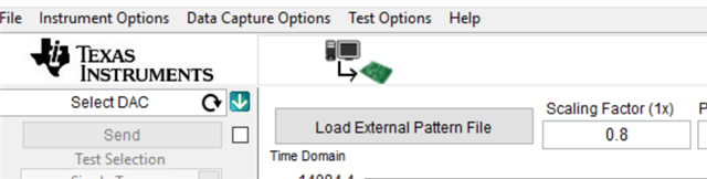
    The adjust the output power of the DAC there are two ways. The first is to adjust the amplitude of the tone the FPGA is sending. This is controlled by the 'Scaling Factor' setting in HSDC Pro. The other control is that you can modify the Tx channels DSA, digital step attenuator, using the following function in the Latte command line: CAFE.setTxDsa(0,txChNo,DSASetting). 

    Regards,

    David Chaparro 

  • Hi David,

    Kindly share the information on how to perform ADC CALIBRATION i.e., DSA calibration.

    Regards,

    Mithuna

  • Hi Mithuna,

    Inside the AFE79xx secure folder, link below, we have a calibration procedure document that can be followed. The document is called "AFE79xx_RxDSACalibrationProcedure" and is in the Application_Notes folder. 

    https://www.ti.com/secureresources/ 

    Regards,

    David Chaparro 

  • Hi David,

    I tried the Latte command line as suggested by you for adjusting the output power. But it seems to be not working. The output power that I have obtained with a scaling factor of 0.9 is around 0.88 dBm. I have added the line CAFE.setTxDsa(0,0,10) after the command sysParams.txNco0 and run the code. But the output power level doesn’t have any change. I am getting the same 0.88 dBm output power.

    Kindly suggest a solution for this issue.

    Regards,

    Mithuna

  • Also kindly share the following information also.

    What will be the expected DAC output power level for the scaling factors ranging from 0.1 to 1.

  • Hi Mithuna,

    The CAFE.setTxDsa function is for dynamic control of the DSA after device configuration and therefore should only be called after 'AFE.deviceBringup()'. If it is called before it will have not be able to update the DSA settings. Can you try moving the function to after the deviceBringup line? 

    The output power level will be dependent on the output frequency and the losses in the front end network. In regard to the scaling factor you can calculate the tone amplitude you can use the following equation: 20*log(scalingFactor). Ex: for a scaling factor of 0.9 the amplitude you are sending to the DAC will be -0.9dBFS

    Regards,

    David Chaparro