Part Number: TIDA-00917
Tool/software:
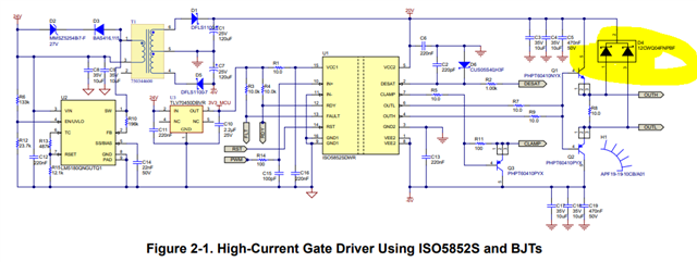
In the TIDA-00917 reference design (https://www.ti.com/tool/TIDA-00917), in order to increase the current capacity of the gate driver ICs, a BJT totem-pole current buffer is used.
I understand that the source/sink peak currents are determined by the external resistances connected in series with the Gate terminal of the IGBT. However, I don't know how to size the base resistors (R5, R6) for the BJTs.
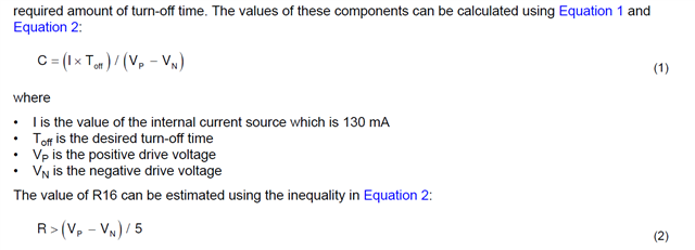
As I understand it, in this application, we want the BJTs to operate in the saturation region, which is considered as a voltage source and hence allows fast charging of the input capacitance of the IGBT. In other words, the active/linear region of the BJTs in the current buffer/booster must be avoided. To achieve this, we will try to reduce their base resistors to ensure that the BJTs always operate in the saturation region for a given gate-source drive voltage.
-
Could you please explain how to calculate these resistors?
-
Moreover, why was a 0.3-ohm resistor (R36) placed between the NPN BJT (Q1) and the driver power supply rail?