This thread has been locked.

If you have a related question, please click the "Ask a related question" button in the top right corner. The newly created question will be automatically linked to this question.

Maximum duty cycle implementation

Part Number: LM5025

Tool/software:

I am trying to undestand how the maximum duty cycle on the LM5025 works.  I currently have a forward converter with a base clock of 200kHz configured using RT and a 225kHz clock being fed into the sync pin with a 50% duty cycle.  What are the requirements on the LM5025 to implement a maximum duty cycle as described under the "Oscillator and Sync capability" in the datasheet?

  • Hi,

    Please read the datasheet. You can search SYNC to get all to your need. The below are my citation of the datasheet. Please have a review. If you have specific questions on the below please let's discuss.

  • Hi,

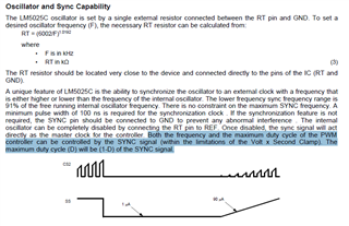
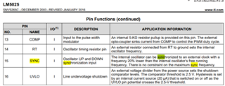
    My confusion comes from the highlighted section of the datasheet shown below:

    Reading this section to me implies that the duty cycle of the signal on the Sync pin will limit the duty cycle of the sync pin, but allows for the duty cycle limit to be over-ridden by the ramp pin setting the maximum on time.  Can the duty cycle of the sync pin impact the maximum duty cycle?

  • Hi,

    Yes, SYNC pulse width will limit the operation max duty cycle. So it is better to set up SYNC pulse width narrower to allow SYNC pulse duty D to have 1-D > converter operational Dmax then the converter Dmax is not affected by SYNC pulse.

  • In my testing, applying a 50% duty cycle sync clock to the sync pin has no impact on the maximum duty cycle.  In my testing with the 50% duty cycle sync signal, I saw the output duty cycle moving from 20%-80% depending on the output of the load and the input voltage.  I did not test outside of this range.

    How does the LM5025 set the maximum duty cycle with the sync pin?  Is there a voltage threshold for this to be enabled?

  • Hi,

    Can you please show the waveforms of SYNC, OUTA and OUTB to help me understand the issue? 

    The datasheet says OUTA Dmax = SYNC (1-D). So SYNC falling edge should trigger OUTA pulse to rise and SYNC rising edge should terminate OUTA pulse.

    If different, then the first thing looks needs to check if OUTA is sync'ed to the external. Can you vary SYNC to increase to 250kHz or 300kHz to see if OUTA can follow SYNC to increase to that? Please also show the waveforms in these cases.

  • Hi,

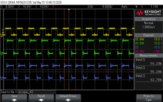
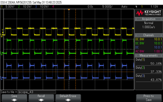
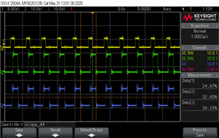
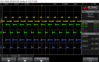
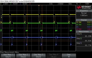
    Below is 4 scope captures showing what I am seeing with the LM5025 in our system.  2 of them have 50% duty cycle and the other 2 have 25% duty cycle on the sync clock.  The first 2 use the sync clock and the only difference is the input voltage on the converter.  If the duty cycle limit is (1-D) of the sync clock, there is no condition where the clock should be able to go above 50% in these first 2, but the duty cycle is reaching 60%.  The last 2 show a the same conditions as the first 2, but with a 25% duty cycle sync clock.

    The behavior of the first 2 do not match my understanding of the behavior described in the datasheet.

    Ch.1 is the sync clock

    Ch.2 is out A

    Ch.3 is out B

  • Hi,

    Is it possible OUTA D = 60% is just due to tolerance when SYNC 1-D = 50%?

    Can you try SYNC 1-D = 75% then to check if OUTA D can be > 60%?

    It looks this is a description not a spec so there can be some tolerance associated.

  • Hi,

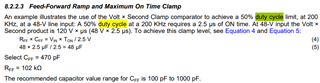
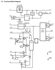
    Also note the block diagram, it shows you still need to set up RAMP properly to make correct duty cycle clamp through Max VxS clamp. The block diagram shows SYNC does not have effect to VxS clamp comparator so the block diagram shows max width pulse terminate still needs max VxS comparator.  

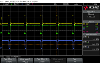
  • I understand that the max VxS clamp can reduce the limit of the maximum duty cycle when setup correctly.  As I understand the datasheet, the sync clock can set the switching frequency and the maximum duty cycle.  How does this limitation work?  Below are 2 scope captures with the input voltage off, just the IC powered.  1 with sync clock at 90% duty cycle, 1 with 14% duty cycle.  Both have the same duty cycle on both out A and out B.  Based on this, as far as I can tell, the sync clock has no impact on the maximum duty cycle.

  • Hi,

    SYNC needs to set up to allow VxS clamp. The block diagram shows SYNC cannot affect VxS clamp comparator. So I think the datasheet means to set up SYNC along with VxS clamp so VxS clamp can work properly. It means, SYNC has to allow enough time to trigger VxS clamp in order to achieve VxS clamp comparator function. As, again, the diagram shows SYNC cannot clamp VxS and SYNC behaves similar to clock to set S-R flip-flop.

  • Hi,

    It is my understanding that the VxS clamp can only set the absolute maximum duty cycle and is part of the feedback loop.  To use the Sync clock to set the maximum duty cycle, you have to disable the internal oscillator instead of leaving it functioning as a redundancy in case your sync clock fails, and you want the unit to keep work.

    Thanks for the help.