


Other Parts Discussed in Thread: TINA-TI
Tool/software:
Hi All,
I'm working with the TINA-TI Transient Reference Design (https://www.ti.com/lit/tsc/snvm022) and am getting alarming voltage output at the HG pin driving my FET, even on the default. The datasheet suggests the absolute maximum voltage for the HG pin is BOOT + 0.3V and the minimum is -0.3V, both with respect to the SW pin.
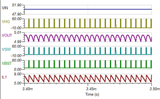
The graph above is the output from the default setup of the transient reference design. HG hits -10V during the inactive portion of the duty cycle every time. Is it safe to assume this is a liberty taken with the sim model to ensure the N-MOSFET is driven completely rather than this output being reflective of actual performance?
Thanks!
