


Tool/software:
Hi team,
Continuing here as per discussion on email.
Could you please provide feedback on the following problem we received from the customer:
Yes, PMP40988 firmware is from DPSDK and also when tried flashing for different labs, it is observed that
For lab4, TTPLPFC_LAB =4 maps to TTPLPFC_lab.enum_lab = 3 as
For lab1, TTPLPFC_LAB =1 maps to TTPLPFC_lab.enum_lab = 0.
Also, since flashing is successful now HV testing is started in lab3, lab4 with AC grid connected at the input and High voltage Power supply board with constant voltage is connected as load and following main issues are noticed.
Lab3:
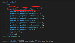
- From Setup & documentation when TTPLPFC_pwm_SwState.enum_pwmSwState is changed to pwmSwState_normalOperation, in watch window the variable is changing to 1 however the value declared for normal operation in ttplpfc.h is 0. Confirm if this is OK?
2. When followed the exact process mentioned in ‘Setup & Documentation’ for Lab3, with 50V rms Input and 100V constant voltage, Power transfer to DC_link capacitors is done with input current 14A rms & Output current 10.11A DC.
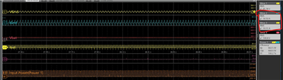
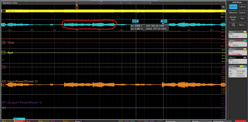
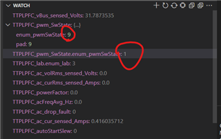
3. However if the same procedure is repeated for any other input grid voltages and different constant voltage loads, No power transfer is done and input current is changing as shown below and also TTPLPFC_pwm_SwState.enum_pwmSwState is changing to value 9/5 in watch window rather than staying at 1 like in the before step. I have tested with grid votlages-120V, 230V and loads of 220V, 350V, 400V. Please confirm if test procedure needs to be modified and if so how.
Lab4:
- Even after following the same procedure mentioned in ‘setup & documentation’ with input 230V rms and Output 400V constant voltage load, inconsistency of Swstate is detected as highlighted
.2. Also transients in the input and output current is observed leading to switch off of system test bench completely. How to proceed further with lab4.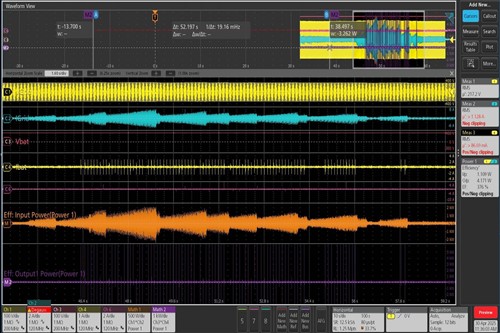
Requesting to kindly confirm if any modifications in the process mentioned in setup & documentation of Lab4/Lab3 needs to be considered while working through-out the input and output voltage range.
Thanks and kind regards,
Akhil & Daniel