This thread has been locked.

If you have a related question, please click the "Ask a related question" button in the top right corner. The newly created question will be automatically linked to this question.

PMP6024: UCC28811DR statrup

Part Number: PMP6024
Other Parts Discussed in Thread: UCC28810, , TIDA-010951

Tool/software:

want to develop 56 Watt singe stage PFC LED driver using UCC28810.

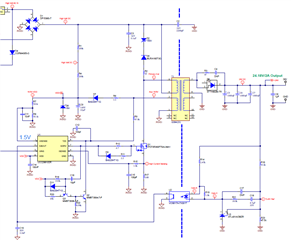
I come across Two designs, PMP6024 & "TIDA-010951" in both designs UCC28810/11 part used for inge stage PFC LED driver. 

But control circuit of TIDA-010951 is much simpler than PMP6024. 

I have few quesries on below designs.

Query : 1

Why here used Mosfet based startup, why can't we go for standard Resistor devider based startup given in the "TIDA-010951"

Which option is prepferable? Also Why Q5 in the "PMP6024" design is ground through D12?

Query: 2

Need to understand the significance of below circuit.

Query : 3

If dimming is not use still this circuit of D18, D16, U4 &D19 is needed? Need to understand the significance of below circuit.

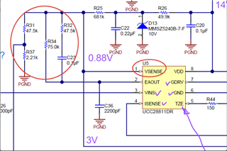
Can we go with the simple option like TIDA-010951 mention below.

  • Hello Sagar,

    I will get back  by  end of the day.

    Regards

    Dushyanth SR

  • Hi Sagar,

    Regarding Query1

    With only resistors start up time is slow,  as it charges from the line voltage with resistors in series and there  is a   power consumption from line voltage. 

    With mosfet it help to charge the VDD caps   faster and  turns off when VDD voltage reaches 18V, we have 18V zener tied to gate of the FET so Vgs becomes

    close to zero.  FET based charging helps in charging VDD faster and reduce the standby power  during run.

    Regarding query2  and query3 

    Both queries are connected. 

    You can see  C36 2200 pf is connected. As this  is PFC,  voltage loop should be slower  , so in TIDA design  2.2uF is connected. But with the TIDA design you  can see Vsense is connected  to VDD divider , if there is OVP in output , it   takes longer time to shut down due to VDD cap and also when Vsense crosses the threshold  , error amplifier inside sink 10uA current out of 2.2uF cap results in slow discharge  and this   results in little slower  shutting down the pwm as a part response to OVP. 

    Circuit you mentioned in Query3 is used for fast OVP response, as it sensed directly from the aux winding and fed to VS.   When Vsense  crosses threshold it sinks 10uA current with 2200pF and Error amp  output voltage falls quickly  and PWM shuts down quickly. 

    This ckt is used to slow the voltage loop as only 2200pF is connected to EAOUT.

    You can use TIDA design if you do not consider  fast OVP response and fast  start up of the controller.

    Regards

    Dushyanth SR

  • Thanks for the detail explanation Dushyanth!

    What is the role of R26, D13 and R25 in the circuit?

  • Hello Dushyanth,

    Any update on above query?

  • Hi Sagar,

    R26 is used to limit the current to D13 and  to drop the enough voltage to clamp the D13 zener to 10V 

    10V x (R31+R37)/(R31+R37+R25) =0.68V

    0.67V is threshold for enabling during the run condition.

    Regards

    Dushyanth SR