This thread has been locked.

If you have a related question, please click the "Ask a related question" button in the top right corner. The newly created question will be automatically linked to this question.

PMP23377: Differing protection circuitry on LMG3100s

Part Number: PMP23377
Other Parts Discussed in Thread: LM5177

Tool/software:

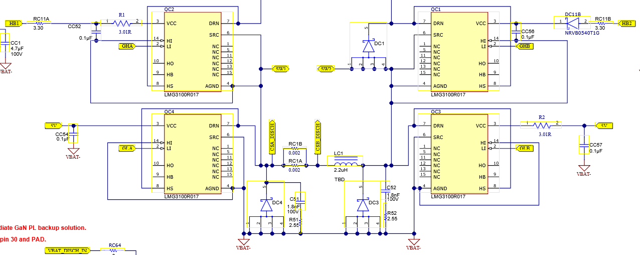
On the reference design the supporting parts for each gan are different and I am having trouble figuring out why. I was hoping you could clarify why this was done.
What purpose does DC11B serve?
Why does QC1 have a diode and a RC filter on its VCC Pin, but QC2 has an RCR filter and no diode on its VCC.
Why is QC2 the only GAN with no drain to source diode.
Why does QC3 have a RC filter on its VCC input but QC4 just has a bypass Cap.

Thank you,

Leo

  • I wanted to follow up this post as it has been a while.

  • Hello Leo,

    Apologies for the delay here. Our internal thread assignment system did not properly set the organization for this thread so it got lost, thank you for starting a second thread to raise the issue.

    I am working with the engineer now based in Taiwan who made this reference design to understand the specific design decisions for each GaN FET. Please allow until early next week for a follow up

    Thanks,
    Zach S

  • Thank you for your speedy reply. 

  • Hello Leo,

    Your questions are focused on two main topics: VCC diode/cap/res and SW diodes. I will answer with those two categories

    VCC circuitry
    Some of the components are leftover from a previous design, which I got clarification about after speaking with the designer of this board
    - RC11A
    - DC11B & RC11B
    So these are not needed and can be removed from the board. But that still leaves another question: Why does QC2/QC3 have VCC resistors but not QC1/QC4?
    The answer is related to slew rate control. for LMG3100, the FET turn-on slew rate is set by connecting a resistor in series with the VCC pin. That is the function of R1 and R2.
    These FETs QC2/QC3 are hard switched FETs (QC2 is high side in buck mode and QC3 is low side in boost mode), meaning the slew rate control resistors will have very significant impact on the slew rate. you can think of these resistors like slew rate resistors for discrete FETs, since they have the same function
    QC1/QC4 are soft switched, so the slew rate will be much more dependent on the system rather than slew rate control resistor, so adding resistors to VCC here is not needed

    SW diodes
    These diodes are all placed to help protect the LM5177 controller from over or under voltage spikes, although some are not needed.
    - DC4 limits the 3rd quadrant voltage during buck dead time. This will keep the SW node ~-0.7V, keeping it safe for the LM5177 controller. The board can be tested without the diode also, and see if the controller can handle higher -ve voltage. This is the most important diode.
    DC3 – limits -ve voltage on the switch node w.r.t GND – again to protect the LM5177. If the layout is good, this diode may not be needed.
    - DC1 – to limit the 3rd quadrant voltage during boost dead time, to limit SW node voltage overshoot over VIN. LM5177 might be able to handle SW more than VIN or not. Most likely this diode is also not needed.
    - QC2 does not need diode – for the buck converter high side there’s no third quadrant operation

    This hopefully helps clear up the design choices here. Please let me know if you have any follow-up!

    Thanks,
    Zach S