


Tool/software:
Hello,
I am designing a precharge circuit using this reference design. I used the calculator to select the components and have the following schematic:
In my application, the battery has a max voltage of 125VDC. I have also attached the calculation sheet I used for reference.
ACTIVE-PRECHARGE-CALC_14-0-0.xlsx
I built a PCB and did some initial testing at 80VDC.
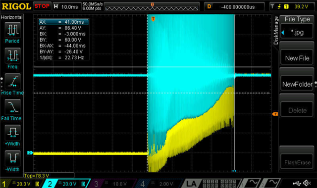
Built two new boards and started testing at input voltage = 80VDC. 2mF cap was used as load.
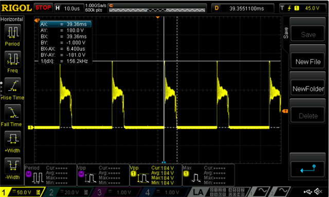
Significant ringing was observed at the switch node.
At 80V input the peak volatge seen at the FET drain was ~180V. The rating on the selected FET is 150V.
The precharge time was ~45ms. Which is great.
Channel 1: Voltage across 2mF Cap measured between J5-J2.
Channel 2: HV input measured between J1- J2.
Channel 1: VDS across FET at 80 V input
 .
.
Is this expected behavior? Should I select different MOSFETs and diodes (higher voltage rated). Also I was wondering what the expected behavior of teh IC was under a short circuit event. The datasheet does not talk about this.

