TIDA-01238: Adding Common-Mode Capacitor

Part Number: TIDA-01238

Tool/software:

Hello,
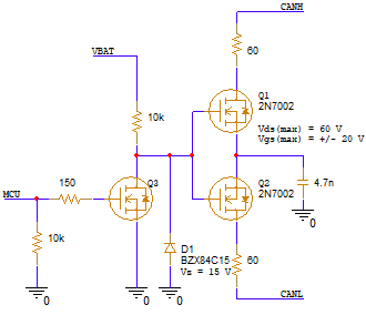
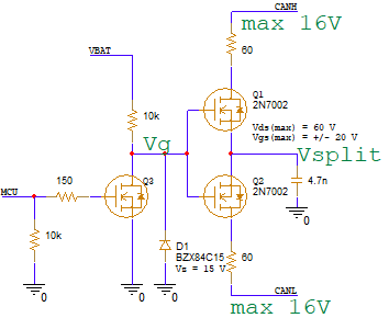
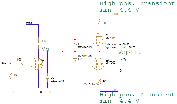
Is it possible to add a Common-Mode filter capacitor in combination of selectable resistors? For example, as in the following circuit.

However, to protect against a short to the battery in automotive applications, the Vgs of the MOSFETs in series with the termination resistors should be ±20 V. In addition, the drive level should be low, but this combination of requirements is not met with standard MOSFETs. Is there any other method to add this capacitor?

  • Hi Sayyid,

    I would recommend to use the photorelay option instead, and make the split termination switchable by connecting the photoMOS between Csplit and GND. When ON, the cap is connected to GND, when off the cap is disconnected and the bus just sees the resistive split, Or placing the phtoMOS between the Csplit node and system GND to turn on and off the entire split termination.

    I.e., the parts are typically rated > 60 V with isolation on the control side. Hence, VGS stress during short to battery should not be a concern as the documentation clarifies the solution as the wide common-mode range option, thanks.

    Best Regards,

    Michael.

  • Hi Michael,

    Using an optocoupler solution requires two components, which increases cost. Its primary drawback, however, is its high and widely varying on-resistance. This variation prevents the bus's common-mode voltage from remaining stable at 2.5 V during the CAN dominant state. Consequently, the split capacitor loses its functionality and cannot effectively stabilize the common-mode voltage.

    Best Regards

    Sayyid

  • Hi Sayyid,

    You may avoid your primary concern by avoiding placing the relay in series with one of the split resistors. Rather, place the relay in series with the cap. Hence, Ron should affect the AC impedance and not the DC bias at 2.5 V I.e., the split resistors will set the common mode DC level. The split cap value may also be increased to meet target levels; C_split = 1 / (2 * pi *(target_impedance - Ron) *f ). Where f = 1 / data rate in mbps.

    For your cost concerns, the schematic shown may work but not confident it will be safe for harsh automotive environments since the gates are not floating with the split node. Hence, during short to battery shorts, the FETs may see excessive / undefined VGS and may not get a stable Ron. Hence, would recommend to ensure their gates are rather referenced to the split node and floating with the bus common mode. This way, the gate driver and split node moves together and VGS always controlled to be within the ratings for a lower risk, to prevent damages.

    I.e., remove the 3rd FET+ the 10 Ks + the 150 ohms and replace with a small isolated gate driver whose return is referenced to the split node and the output tied to the gates of the two CAN FETs. You may add additional system protection such as a TVS diode, thanks.

    Best Regards,

    Michael.

  • Hi Michael,
    Placing the switch in series with only one resistor caused imbalance at the midpoint and I think it is nonfunctional. Adding a switch in series with the capacitor provides no benefit, since the capacitor is required whenever the terminations exist and disconnecting it is unnecessary.

    Using an isolated gate driver could address the severe overvoltage issue, but it increases cost. Maybe a possible alternative is adding protective TVS between gate–source and drain–gate to mitigate the problem.

    Best Regards

    Sayyid

  • using 60 V MOSFETs, driving them by VBAT instead of 5V and adding a 15 V Zener on the gate of them as protection may solve the issue.

  • Hi Sayyid,

    It would seem shorts to battery can still drive the VGS above ± 20 V beyond the single 15 V clamp (especially during negative transients). And a bidirectional gate to source clamps should be more suitable. However, you may still need to account for leakages, timing, and variabilities with careful series gate limiting.

    Hence, you may consider the back to back N-MOSFETs in series (tied source-to-source) so the body diodes do not conduct, bidirectional TVS from gate to source on all FETs + a small series gate resistor up to 100 ohms, thanks.

    Best Regards,

    Michael.

  • Hi Michael,

    Based on the Zener diode datasheet, its maximum clamping voltage at IZ=5 mA is about 15.6 V. Therefore, the gate voltage Vg will be between approximately 15.6 V (slightly higher during transient pulses where IZ>5 mA) and –0.7 V under any condition, including transient voltages at VBAT.

    For the CAN bus, the maximum voltage on CANH and CANL under a short-to-battery condition is 16 V. Additionally, in the capacitive coupling clamp test—applied to the CAN bus as with other automotive signal lines—it seems unlikely that the bus voltage would increase further, since termination resistors and split capacitor (at least on one node) prevent this.

    Given these constraints, under what condition do you think the MOSFET’s Vgs could actually exceed 20 V?


    Best Regards

    Sayyid

  • Hi Sayyid,

    Best Regards,

    Michael.

  • Hi Michael,

    I modified the circuit based on your comments. The high positive transient only affects the Vds of the termination series MOSFETs, not the Vgs, correct?. However, a negative voltage on the CAN line (–4.4 V) can cause a higher voltage across Vgs, which should be prevented by placing a TVS between Gate and Source. Therefore, what is the necessity of using a bidirectional TVS across Gate–Source? Also, what is the main reason for the –4.4 V, since the document you sent only describes high transient voltages?


    Best Regards

    Sayyid

  • Hi Sayyid,

    Given these constraints, under what condition do you think the MOSFET’s Vgs could actually exceed 20 V?

    Please note that the feedback are for examples to your question - a negative swing on CAN bus of - 4.4 V can make VGS exceed the ± 20 V limit I.e., gate is clamped at 15.6 V while source driven to 15.6 V. VGS = 15.6 - (-4.4) as 20 V. Under such a condition or slightly larger spikes or if IZ > 5 mA, the 20 V may be exceeded. Hence, the recommendation for limiting both polarities with a bidirectional TVS as the ones used would mainly clamp the positive gate voltages, thanks.

    Best Regards,

    Michael.