Other Parts Discussed in Thread: UCC21710-Q1
Tool/software:
Dear Team,
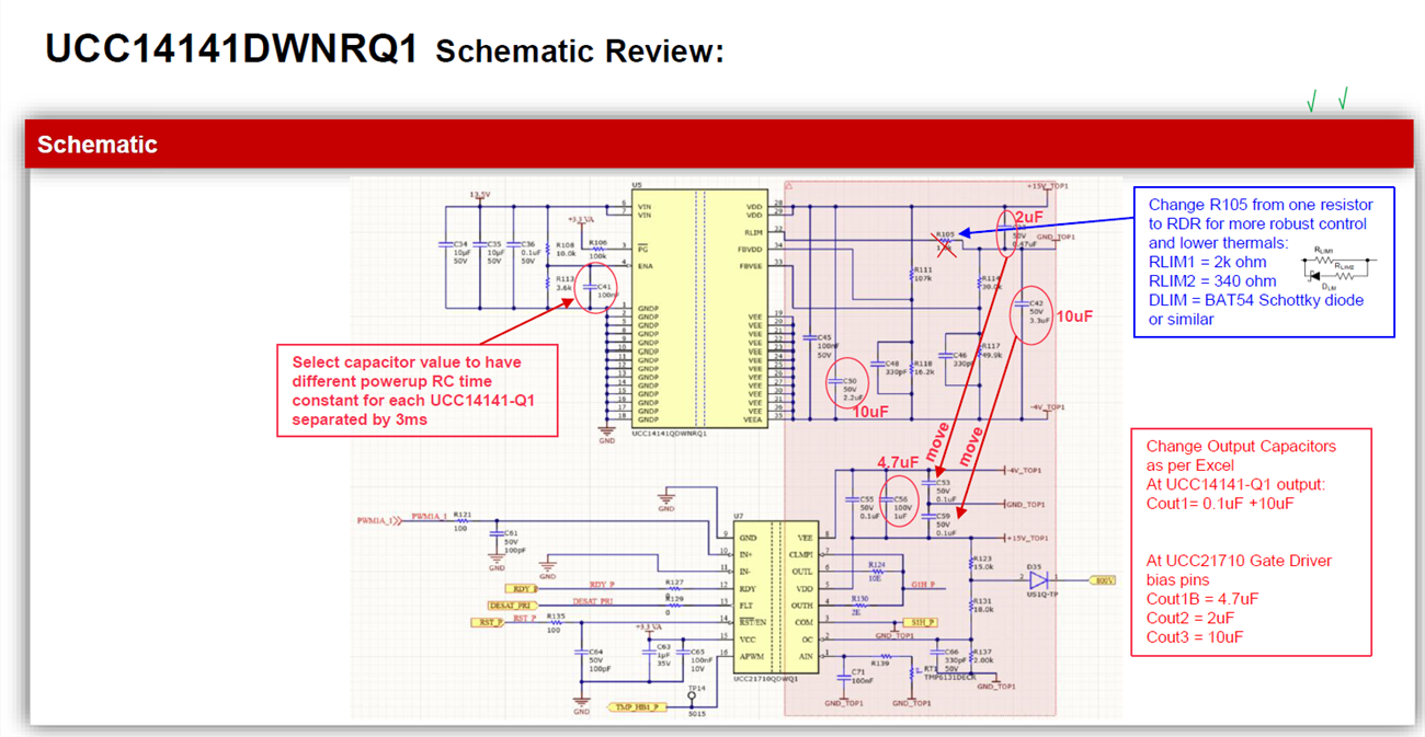
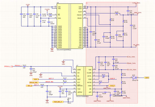
We are using the UCC21710-Q1 gate driver in a DC-DC converter with a full-bridge topology. The gate driver is powered by a UCC14141QDWNRQ1 DC-DC module, which provides +15V and -4V. The main switches are IPTC011N08NM5 SiC MOSFETs.
We are experiencing a consistent issue where the gate driver shuts down when the DC input supply voltage exceeds approximately 170V. This behavior is unexpected, and we have taken several troubleshooting steps without success.
Key Design and Observations:
-
Gate Driver Power Supply: The UCC21710-Q1 is powered by the UCC14141QDWNRQ1 module.
-
Protection Features: We have disabled the overcurrent (OC) and analog input (AIN) pins by tying them to GND. The APWM pin is floating. We also removed the D35 diode to disable drain voltage sensing.
-
Gate Resistors: The gate turn-on and turn-off resistors are 10Ω and 2Ω, respectively.
-
Troubleshooting: We've observed that changing the R_LIM resistor on the UCC14141QDWNRQ1 from 75Ω to 133Ω allowed the input voltage to reach 175V before shutting down, but we are unable to go higher. This suggests the issue may be related to the power supply's current limit.
We have attached the relevant schematic images for your review. We suspect the shutdown is due to an undervoltage lockout (UVLO) condition on the UCC21710-Q1, potentially caused by the power supply struggling to maintain a stable output at higher input voltages.
Any guidance you can provide on this matter, especially related to potential power supply instability, ground reference issues, or other protection mechanisms, would be greatly appreciated.
Thank you for your time and assistance.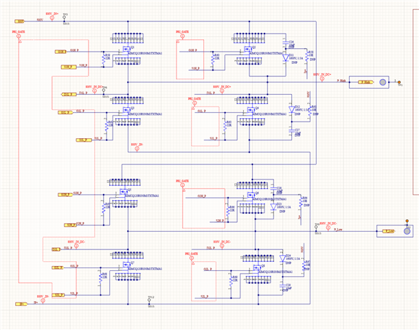
Ajay S Ruli
Systems Engineer- ALTEN GT