PMP11282: Support Required: Support Required – Issue with PMP11282 Rev A Reference Design

Part Number: PMP11282


Tool/software:

Dear TI Team,

I am working on the reference design PMP11282 Rev A, which is implemented on the PMP11064 Rev B PCB. I am currently facing an issue with the LLC IC UCC25600D, where it is not regulating properly at startup.

For testing, I am applying an input voltage of 80–90 VAC, 50 Hz.
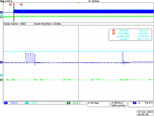
The LLC half-bridge resonant converter is designed for a 24 V regulated output, but I observe that the output initially rises to 32 VDC and then gradually reduces back to 24 VDC. At this stage, only the output capacitors are connected, and no load is applied.

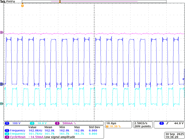
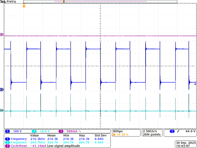
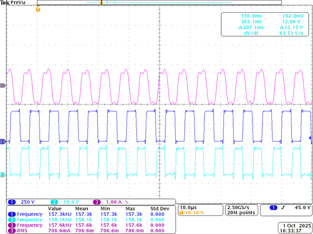
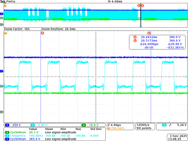
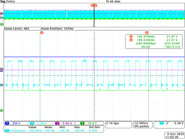
  • Blue signal: Output voltage (~375 VDC)

  • Yellow signal: Output voltage (initially 32 V, gradually reducing to 24 V)

Could you please confirm how much minimum load is required for stable regulation? Also, I would appreciate your guidance on how this issue can be resolved.

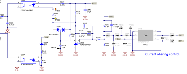
Please find the schematic and DSO waveform photo attached for reference.

Best regards,
Anand Matta


 8424.400 Watt Half Bridge LLC.pdf

  • Hi Anand,

    Can you confirm if you are using the same magnetics as I used in PMP11282? I did no load test and no overshoot at the output was observed. Please refer to PMP11282 test report. Also, the circuit (D506, R539, C536) will smooth the startup ramp to prevent overshoot.

    In short, there might be some mismatch between the PMP11282 design and the board you are testing.

    Regards,

    Sheng-Yang Yu

  • Dear Sir,


    Yes, I have used the same reference design as PMP11282.

    In comparison with the test report, I observed the following:

    • My PFC output is regulating at 375 VDC, whereas the test report shows 384.02 V.
    • My output is regulating around 20 V at 3 A load, whereas the test report shows 24.023 V.

     Can I try making D506 DNC and test the circuit?

     Additionally, I sometimes face startup issues on my PCB. Occasionally, it does not start properly and only gives about 6 V output, even though the PFC is regulating at 375 VDC.

    For reference, here are the auxiliary (net names as per PMP11282) measurements on my board:

    • 12Vs Net: 14.35 V
    • 5Vs Net: 4.967 V
    • 6V Net: 6.515 V
    • 12V Net: 14.10 V

    Please advise if the mismatches could be related to the startup circuit or if further tuning is required.


    Best regards,
    Anand Matta

  • Yes, you can try to DNP D506 to compare. Also, you should check transformer primary winding current to observe it's current level and operational frequency when you stuck at 6V. Is it hitting over current threshold?

  • Dear Sir,

    Please find attached the DSO screen captures for the following scenarios:

    1. Output at 20 V with load – Operating frequency observed: 162 kHz
    2. Output at 32 V without load – Operating frequency observed: 344 kHz
    3. Output at 6 V with load – Observed that the low-side MOSFET is not switching

    In each case, I have measured the transformer primary winding current along with the switching waveforms of both the high-side and low-side MOSFETs. I did not observe significant deflections in the primary current waveform.

    Kindly review the attached results and advise on possible causes or next steps.

    Best Regards,
    Anand Matta


  • The current doesn't make sense to me. You should see sinusoidal (heavy load) or triangle (light load) current shape. You need to find out why the current isn't as expected. 

  • Dear Sir,

    Please find attached the DSO images with the current probe.
    Earlier, I had captured the wrong channel.


    AC input current: ~0.3 A (measured with clamp meter, before bridge rectifier)

    DC output current: ~1.4 A @ 20 V (measured with clamp meter)

    Kindly review and advise further.

    BR,
    Anand Matta

  • Hi Anand,

    The waveform with load (20V) looks good to me. One possible reason for higher output at no load is the transformer and output rectifier parasitic capacitor is high causing the converter becomes uncontrollable. You might want to check if the winding stack up of the transformer causes the high intra-winding capacitance. Or the parasitic capacitance of the synchronous rectifier is higher than the original design. The other possible reason is that the opto-coupler U503 CTR ratio isn't high enough. Therefore the output voltage goes higher in order to provide enough current for the opto-coupler.

    For the 6V output low-side FET not switching issue, you need to check the waveform while low-side FET is still switching. It is better if you can monitor the moment right before low-side FET not switching to see what protection it triggered to stop FET switching. 

  • Dear Sir,

    Thank you for your detailed analysis and suggestions.

    Regarding the optocoupler, I used TLP785GB (CTR range 50%–600%) in place of PC817X4NSZ0F, as the original part was unavailable. I hope this substitution is acceptable and not contributing to the issue.

    For the 20V output, the converter maintains regulation under load; however, our target design voltage is 24V. Could you please advise why it may be limiting at 20V instead of reaching 24V under load conditions?

    Regarding the 6V output, I have observed that if the converter is powered on with no load and then the load is connected afterward, it operates correctly. However, if started with load already connected, the low-side FET stops switching. I will further capture waveforms around the point just before the low-side FET stops switching to identify the protection mechanism triggering this.

    Thank you again for your support and guidance.

    Best regards,
    Anand Matta

  • Hi,

    The optocoupler CTR range I selected is 300%-600%. 50%-600% is too wide of range to cover. You need to find a part that has the same CTR range as in the original design.

    I found another part should work in Digikey stock.

    https://www.digikey.com/en/products/detail/onsemi/FOD817DSD/1050227

    Please replace Optocoupler first to see if the situation changes.

  • Dear Sir,

     Please find the attached schematic for your review.
    Kindly let me know if any changes are required.

    TI Reference.pdf

    The output feedback loop appears to follow a Type III compensator design; however, I noticed that the 21.5 kΩ resistor in parallel with the 2700 pF capacitor are additional components.

    Could you please share the calculations for the pole and zero frequencies, along with the corresponding feedback component values (R515, C100, C529, C530, R534, R526)?
    Please find the attached screenshot for reference. 

    Also, could you clarify the purpose of the current sharing control—is it intended for parallel operation, constant current (CC) mode, or overcurrent shutdown?

     BR,s
    Anand