UCC28710: UCC28710 Simulation Not Working

Part Number: UCC28710


Tool/software:

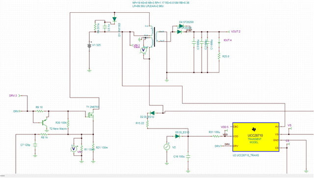
I have designed an AC/DC charger with specifications of 54V / 200W for a battery bank. An open-loop simulation was carried out without implementing Primary-Side Regulation (PSR), and the expected output was obtained. The corresponding simulation file is attached for reference. 

Battery charger - autosave 25-09-10 18_56 (1).TSC

But when I try to run the closed-loop simulation, the DRV signal is not generated. The corresponding simulation file is attached for reference. 

Battery charger with feedback - autosave 25-09-11 10_42.TSC

Please suggest the possible reason and solution for this issue.

Regards,

Kalyani

  • Hello,


    If the DRV signal is not present it is possible that you have an input under voltage fault causing the DRV from working properly.


    At power, up the UCC28710 will give three sample pulses looking for input voltage.  If the input voltage is lower than programed input under voltage lockout the DRV pin signal will terminate and the VDD pin will fault cycle. This mill look like the DRV is doing nothing.  If the VDD pin is not allowed to cycle the part, the part will stay latched off and you will not have a DRV signal.  I think this is what may be wrong with your simulation.


    The following link will bring you to an application note that has a section on input UVLO that the UCC28710 uses.  I believe this information will be helpful in troubleshooting your simulation.

    https://www.ti.com/lit/pdf/sluaac5


    Regards,

  • Hello Mike O,

    Thank you for your response.

    I think the OVP condition is not the cause of the problem, since the VS pin voltage is 4.6 V (well within range). Also, the VDD pin is supplied with 25 V, which is higher than the UVLO turn-on threshold.so the controller is enabled. However, only a single drive pulse is observed, after which the DRV output stops no DRV pulses are generated.

  • Hello,


    If you have the VDD pin set at 25 V and a fault is triggered it will not reset under a fault and latch the drive off.  That is discussed in the mentioned application note.  You need to come up with a way of power VDD where it can cycle between Vdd(on) and Vdd(off) if a fault should occur.


    I am surprised that you are only seeing one driver pulse.   They generally come in an interval of three packets and can be as much as 1 ms apart. You might want to check this to see if you are getting 3.


    The other thing I am wondering is if this is a sampling issue.  Try increasing the number of samples an rerun your simulation.


    Regards,

  • Hello Mike O,

    Now the DRV pulse is generated, but after around 6% of the simulation progress the simulation not working. I have attached my schematic file below for reference. Could you please review the schematic and suggest what could be causing this issue and how to solve it?

    Charger with PSR.TSC

  • Hello,


    I reviewed your schematic and you have a 25 V DC source diode connected to VDD.  This will prevent the design from cycling VDD if it should enter a fault.  The design will just latch.  I would remove that and put an initial voltage of 25 V on the VDD capacitor/s to speed up the startup.

    I would recommend using the excel tool at the following link to check your design.

    https://dr-download.ti.com/design-tools-simulation/calculation-tool/MD-7lA1gsKToi/01.00.00.00/sluc590.zip


    After doing the above if the design still is shutting down.  Study CS, VS, DRV and Vout and look at the last 3 switching cycles before shuts down.  With this information it should be possible to determine if the design is shutting down due to UVLO, OVP or a CS fault.


    Regards,

  • Hello Mike O,

    As suggested, I removed diode but when I put an initial voltage of 25V on VDD capacitor in this condition the controller produced only a single DRV pulse, so I kept the capacitor parameter same as it is.

    Next, I checked the CS, VS, and DRV waveforms. The CS pin voltage is about 780 mV, so no over-current fault is present. The DRV pulses are generated correctly. when talk about VS is not going into UVLO because simulation not running upto 100% hence it show voltage at VS pin below 4.6V it rises slowly. Please refer to the attached image below

    Is there any other issue? Please suggest the possible reason and solution

    Regards,

    Kalyani

  • Hello,


    That is strange that it only has one DRV pulse when the diode is removed.  Can you remove the diodes again and set the initial voltage on the VDD capacitors to 25 V and retake the waveforms that you have shared?


    Regards,

  • Hello,

    Sorry, I removed the VDD supply earlier, so the driver pulse wasn’t generated. In the attached reference design the drive pulse is present, but my simulation stops before it reaches 100%. Any suggestions, please?
    Charger with PSR2.TSC

    Regards,

    Kalyani

  • Hello,

    There might be something wrong with the model when the VDD is latched at 25 V.  I would try using the V2 piece wise liner model in the released tool.  This will give you a faster startup and may remove the issue that you are having.


    If that does not resolve your issue it might be worth while to start with the released debugged model.  Then modify it to your design requirements.  This may save you time in the debug process.


    Regards,

  • Hello,

    I I have already taken both the IC SPICE model and the V2 piece-wise linear model from the reference design shown in the image above. 

    Regards,

    Kalyani

  • Hello,

    The simulation is now running correctly, and I am getting the expected results. However, during the short-circuit test, the CS pin voltage does not reach 1.5 V as expected. I have attached my schematic for reference. Please suggest what could be the issue.

    Regards,

    Kalyani

  • Hi Kalyani, There is a  chance that, if you short ckt it, it may start hitting UVLO  and stops generating PWM to get enough primary peak current to reach 1.5V.

    What is the voltage you are getting @CS pin during short ckt.

    Regards

    Dushyanth SR