WEBENCH-POWER-DESIGNER: UCC28C57LDR

Part Number: WEBENCH-POWER-DESIGNER
Other Parts Discussed in Thread: TLV431

Tool/software:

Dear Sir,
1). I'm Using IC "UCC28C7LDR" for my Flyback Converter With the input voltage of 130V DC and Output voltage is of 24V/4A,     
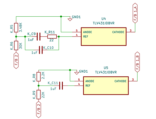
     In the Schematic i have just added the Compensation circuit to Reference Pin which i had Later Changed to Cathode pin of TLV431.
     I Have Referred the Schematic of Webench and i have designed my Schematic by making small Changes.
     I Have Uploaded my Schematic please refer once.

3250.WBDesign8.pdf
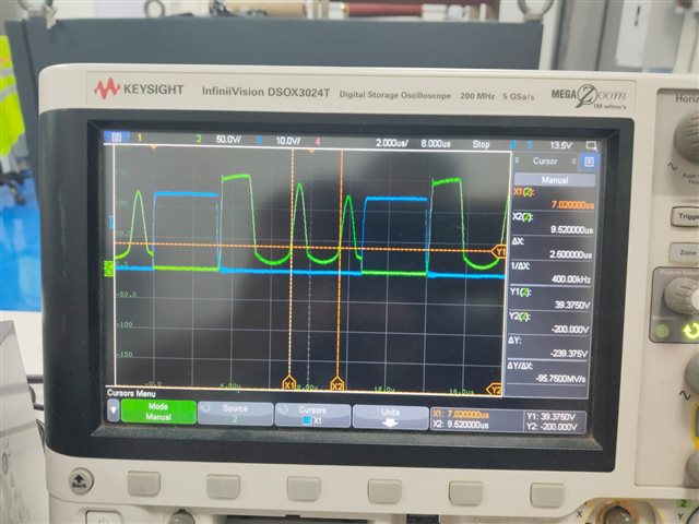
2)  I'm Thinking it is the Compensation Issue Because when Load is Not Connected then as per my Requirement im Achieving all voltages, but whenever I'm Applying the Load then my all Secondary, Auxiliary Voltages all are Fluctuating.  

3) If there is any Excel Sheet for Compensation, please Upload.

4) Is there any Spice Model Available for this IC.

Kindly help me to Overcome this Issue.
AUX_SCHEMATIC V1.1.pdf

  • Hi Chetan,

    Thanks for reaching out.

    Schematic reviews usually take about 1 week. I will review it and get back to you as soon as possible.

    4) Is there any Spice Model Available for this IC.

    No, unfortunately, we do not have any compensation excel files. The datasheet should guide you through the design process.

    4) Is there any Spice Model Available for this IC.

    Yes, please refer to this link on ti.com. PSPICE model for this part can be found in the "Design Tools and Simulation" section on this webpage.

    Thank you for your patience.

    Best,

    Adhvaidh

  • Hi Chetan,

    I did some research on why this might happen. Usually, such scenarios occur when the inductor terminals are reversed. On the schematics PDF you sent, the dots on the transformer are missing. Can you please populate the dots and send it over?

    Thank you.

    Best,

    Adhvaidh

  • Hello Aravind Sir, Thanks for your Response.
    The Dot Notation is Shown in the Image, and also i want to Add one More Image that might add up some value to solve the issue.
    The Blue = Gate to Source Waveform & Green = Drain to Source Waveform; Why Drain to Source Waveform is in this way?.  
    The Primary Inductance of T/F = 470uH, Primary Leakage = 18.2uH. [As per my Calculation, Inductance and air gap should be 470uH and 1mm Gap. But in Practical the Inductance i got is 1.52mH so I increased the gap such that to get 470uH so in this case i got the Pri. Leak Ind = 18.2uH]
    Do you have any Comments on this Sir??
    Here i have Attached 2 Waveform Images  Naming SL.No:-01 & 02.
    Setup Testing: - I have Removed the Start-up resistors and Given the IC Supply From an External 24V SMPS, & the Input DC is Increasing Linearly and Verifying the Output Voltages i have just reached the Output Voltage of 10V (On the +24V Secondary Output Which you can see in the Schematic).
    As I'm increasing the Input DC Voltage then Number of Oscillations are Increasing on the Drain to Source Waveform as shown in the Image (Leakage Inductance is Low & Gate Pulse is Rock Steady but Why it's Happening).


    We Respect your Response, Kindly Comment on this.

    Thank you,
    Chetan BIJAPUR

  • Hi Chetan,

    Thank you for confirmation. I have seen such valley switching behavior at light loads. Anyway, I will check your schematics and will get back to you.

    Thank you for your patience.

    Best,

    Adhvaidh

  • Hi Chetan,

    We are sorry for the delay in response. But yes, as I mentioned earlier, such switching behavior at light loads is not an abnormality. The converter is getting into the DCM mode, and the ringing that you see is due to the resonance between Lprimary and COSS of the FET (tDead period) . 

    For more information on DCM operation, please refer to this video on TI.com- https://www.ti.com/video/5214377648001

    I'm Thinking it is the Compensation Issue Because when Load is Not Connected then as per my Requirement im Achieving all voltages, but whenever I'm Applying the Load then my all Secondary, Auxiliary Voltages all are Fluctuating.

    In your schematic, I noticed that the anodes of both the TLV431s are connected to FB2. Is that desired in your design?

    I would recommend you try removing either U5 or U4, and short F/B 1 and F/B 2 after removing the inductor (L2). That way, we can directly refer the output voltage.

    Then, please adjust your compensation network and get back to us still face this issue.

    Please let us know if you have any questions.

    Thank you.

    Best,

    Adhvaidh