This thread has been locked.

If you have a related question, please click the "Ask a related question" button in the top right corner. The newly created question will be automatically linked to this question.

LMR33630: LMR33630ADDA

Part Number: LMR33630

Good day,
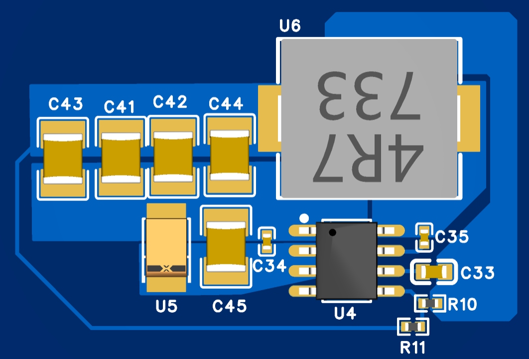
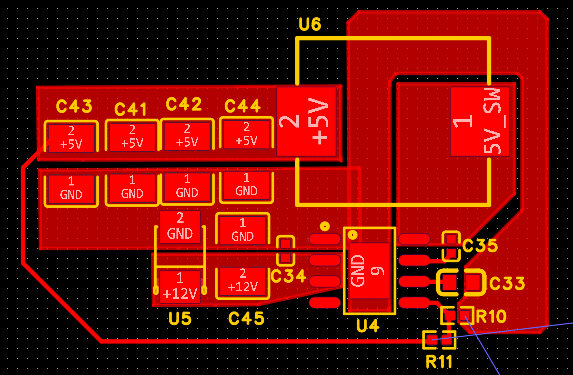
I am aiming for a 5V output with a 12V voltage using the LMR33630ADDA voltage converter. I have designed a PCB as an example; have I done it correctly, what are my mistakes, and what thickness in mm would you recommend I use?image.png
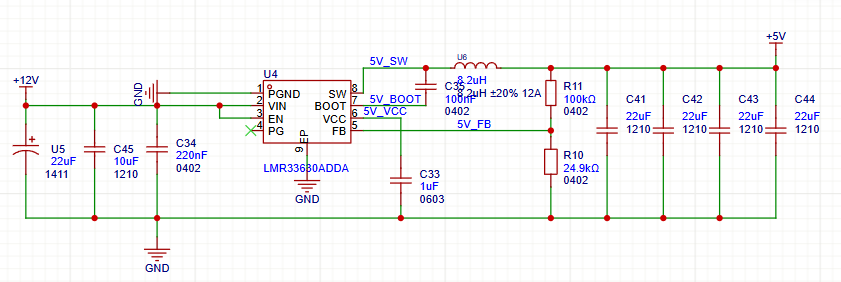
image.pngimage.png

  • Hello

    I will review and provide feedback by EOB on Thur. 3/5/2026 PST.

    Thanks

  • Hello

    Your design looks good.

    Here are a few comments:

    1. Ensure that the output capacitor bank provides at least 40uF to 50uF of capacitance at 5V of D.C. bias

    2. It is prudent to leave a space on the PCB layout for a small capacitor across R11.

    3. It is best to complete the ground plane around the bottom of your PCB image.  This will provide a short ground path 

    for C33.  You can do this by moving the trace from R11 to another layer.

    4. In general, you want as much ground plane on top to provide a good heat sink.  Also, a solid ground plane in the layer

    under the device is recommended.  Ground vias under the regulator are recommended.

    5. Ground vias around the input and output capacitor grounds are reccomened.

    Thanks