This thread has been locked.

If you have a related question, please click the "Ask a related question" button in the top right corner. The newly created question will be automatically linked to this question.

Thermal Simulation PCB Size and Layout

Other Parts Discussed in Thread: LM5118-Q1

Hi,

I have been running a thermal Simulation with a LM5118-Q1 Design.

It is not clear to me what dimensions the PCB structure has that is used per default for this? Where do I see the distance that is used f.e. between the IC and the Diodes?

Also, is it already possible to change the PCB layout / dimensions?

Many thanks,

Katharina

  • Hi Katharina,

    Sorry for the delay. 

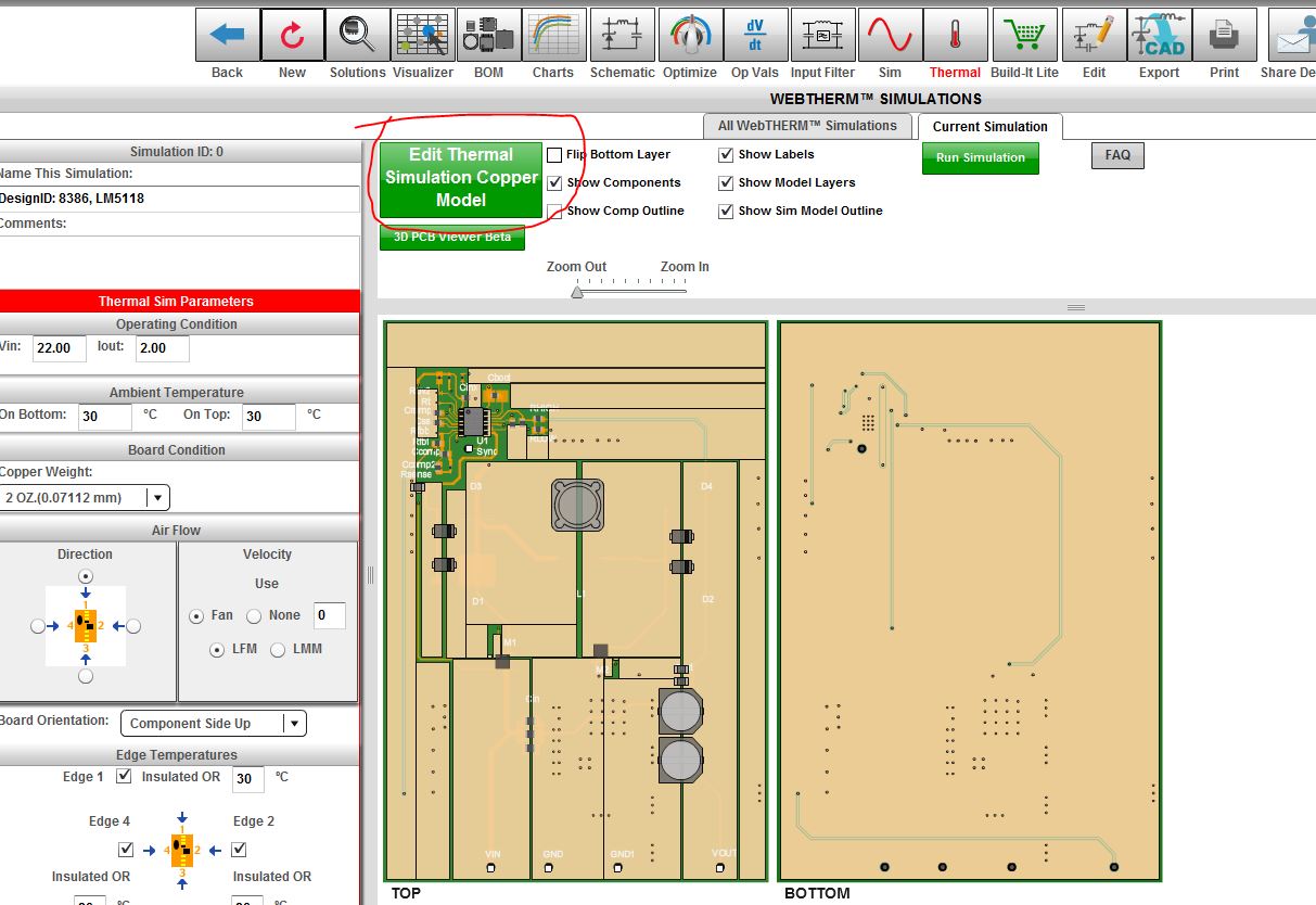
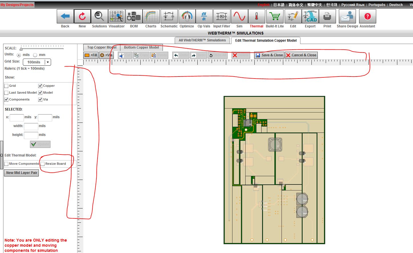
    To see the board size, to change simulation copper and board size, please select "Edit Thermal Simulation Copper model" button within the thermal simulation page (See below).  

    The exportable layout is NOT editable but the simulation layout copper is allowed.  We don't have an user selectable measuring ruler to tell you the distance between two components so you will have to estimate it using the edge rulers.