This thread has been locked.

If you have a related question, please click the "Ask a related question" button in the top right corner. The newly created question will be automatically linked to this question.

WEBENCH® Tools/TPS50601-SP: Issue creating design, duty cycle

Part Number: TPS50601-SP

Tool/software: WEBENCH® Design Tools

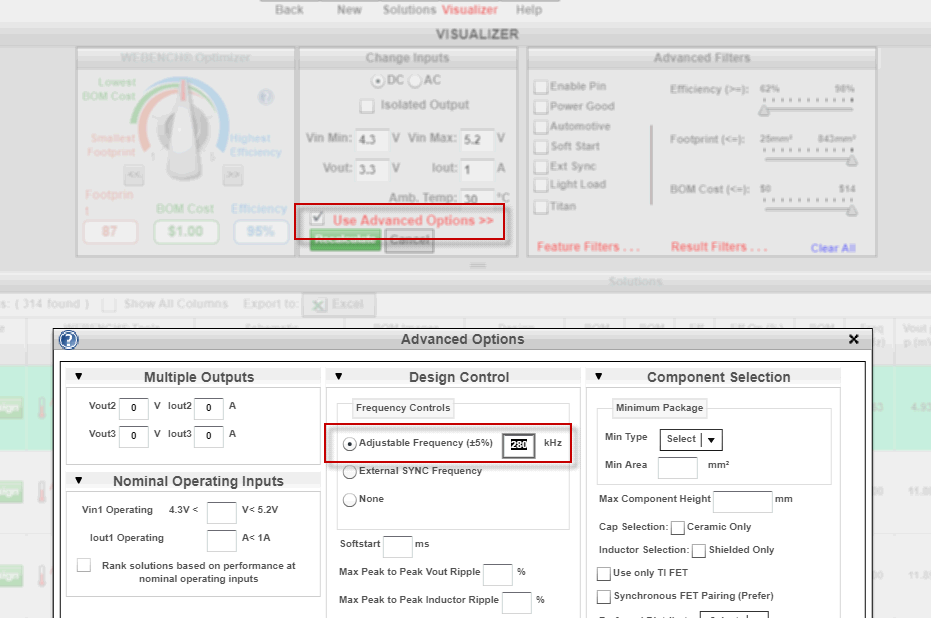
I'm trying to create a Webench design for the TPS50601-SP with the following design inputs: Vin = 4.3 to 5.5V, Vout = 3.3V, Iout = 1A.  

Webench reports it cannot create design and reason given is the "calculated duty cycle is > duty cycle due to min off time".  This reason doesn't make sense.  If I lower the max Vin voltage to 5.2V or 5.0V, the design works fine.  The duty cycle is actually higher with these lower Vin settings.  It seems the device should be able to operate with Vin = 5.5 and Vo = 3.3V (Fsw around 390 KHz). If anything, the low side Vin is pushing the min off time limit due to high duty cycle. 

Is this design input violating some other design parameter? 

  • Mark,

    Yes, this is a bug and thanks for reporting this in detail. I will work on this fix and aim for release this week or early next week. I will let you know once released. For now, the workaround could be to use lower Fsw and specify the value using advanced options. I see for 500ns of min off-time the value is coming out to around 280kHz for dial position 3 for your design.

    Here is a readymade default design for that:  https://webench.ti.com/appinfo/webench/scripts/SDP.cgi?ID=320557081ED76CD4

    Regards,

    Amod

  • Hi Amod,
    Thanks for the quick response and the suggested work-around. This approach works for what I need.