This thread has been locked.

If you have a related question, please click the "Ask a related question" button in the top right corner. The newly created question will be automatically linked to this question.

TINA/Spice/UCC2801: VR2 value

Part Number: UCC2801
Other Parts Discussed in Thread: TINA-TI, , OPA336

Tool/software: TINA-TI or Spice Models

Team,

My customer has the following issue: 

I downloaded the UCCx813-1A.lib model for simulating UCC2801PW.  The value of VR2 inside the unprotected model is missing.  Can you look into that?

Regards,

Aaron

  • Hi Aaron,

    The syntax is perfectly fine for PSpice and TINA-TI (and many other spice simulators). It implies a 0V source connected between node "uvlout" and node "47". The last argument is optional. If it is not specified, it is assumed to be 0V by default. So

    VR2 uvlout 47

    is equivalent to

    VR2 uvlout 47 0

    If you have issues importing it into another simulator, please add the explicit 0 at the end.

  • Nikhil,

    I add “0” to VR2 line in the UCCx813-1 model. It is still not working. The simulation works at 8.85ms. Any idea?

    VR2 uvlout 47 0

    Is there an AC model for UCC2801 or UCCx813-1?  All I can find is the transient model.  Thanks.

  • Aaron,

    It looks like the customer is having a convergence issue in their simulator, since it is running partially. It would be best to have them try this out in TINA-TI. We already have working schematics in TINA-TI which can be used as a starting point.

  • Hi Nikhil,

    Thanks for your response.  I tried the model in PSPICE and it is working fine.  However, our team has to use LTSPICE for the simulation.  Can you give us some hints on how to get this model to converge in LTSPICE?  Is there any convergence tricks you can share?

    Thanks.

    David Lam 

    david.y.lam@Honeywell.com

  • Hi David,

    Unfortunately, we do not have the means to support our models in LTSpice nor are we allowed to do so per their EULA. We work closely with many simulator companies to make sure our models can work in their simulator, but this us usually a close collaboration between TI and the simulator manufacturer. Unfortunately in this case, the situation is a bit more complicated as you can imagine.

    Since the model is unencrypted on the web, one option could be to post your query on the LTSpice forum to see if they can respond to your issue in LTSpice.

    I am sorry, I can not be of more help on this specific issue.
  • Hi Nikhil,

    Inside the UCCx318-1.lib there is a MOSFET parameter "VFB" as shown below. LTSPICE and some simulators don't understand that. Can you suggest a way to mitigate?

    .SUBCKT Si7344DP 10 20 30
    * TERMINALS: D G S
    M1 1 2 3 3 DMOS L=1U W=1U
    RD 10 1 3.51m
    RS 40 3 1.24m
    RG 20 2 0.7
    CGS 2 3 1.15n
    EGD 12 0 2 1 1
    VFB 14 0 0
    FFB 2 1 VFB 1
    CGD 13 14 1.40n
    R1 13 0 1.00
    D1 12 13 DLIM
    DDG 15 14 DCGD
    R2 12 15 1.00
    D2 15 0 DLIM
    DSD 3 10 DSUB
    LS 30 40 2.50n
    .MODEL DMOS NMOS(LEVEL=3 VMAX=41.7k THETA=80.0m
    + ETA=2.00m VTO=1.50 KP=48
    .MODEL DCGD D (CJO=1.40n VJ=0.600 M=0.680
    .MODEL DSUB D (IS=58.1n N=1 RS=0.1 BV=20.0
    + CJO=743p VJ=0.38 M=0.25 TT=50n
    .MODEL DLIM D (IS=100U)
    .ENDS
  • Hi David,

    Sure, I can explain what it is going.

    VFB 14 0 0
    FFB 2 1 VFB 1

    VFB is a 0V voltage source between nodes 14 and 0
    FFB is a current controlled current source. It is measuring the current through the 0V voltage source defined by VFB and reflecting the same current between nodes 2 and 1 (with a gain of 1 -- the last term on that line)

    I would be surprised that LTSpice would not be able to recognize the VFB term. It is a standard voltage source. In your last message, you had mentioned that the simulation ran till about 8ms. That makes me a little skeptical that LTSpice is not recognizing that element (I think it is). Is there any reason why you feel VFB is an issue?

    Moreover, this is just the external FET in the application. If you are not using this FET in your application, you can simply remove that from the lib file.

    I hope that helps.
  • Hi Nikhil,

    Sorry, I got mixed up with another LTSPICE issue. Actually this is with level 3 MOSFET model that use VFB parameter as shown below. Do you have any suggestion to mitigate that? Thanks.

    * MODELS for LEVEL 3 PSpice
    .MODEL PCH PMOS (LEVEL=3 TOX=30E-9 CGDO=1.80e-10 CGSO=1.80e-10 CJ=7.199E-4 CJSW=3.40E-10
    +AF=1.05 KF=1.0e-31 JS=4.0e-7 JSSW=3.0e-13 RSH=117 MJ=.47 MJSW=.16 VFB=-0.34 PHI=0.71 VTO=-.892
    +LD=12E-9 WD=43E-9 TPG=+1 GAMMA=0.6)

    David
  • Hi David,

    I am not able to find this code in the UCCx813-1 model. Can you please point me to the file on TI.com that has this code?
  • Hi Nikhil,

    Actually that is from OPA336.lib I used in the feedback path.  The model is as shown below.

    .subckt OPA336  1 2 3 4 5
    *
    M61      4 64 55 55  PCH W=20U L=0.8U     M=1 
    M59      55 53 3  3 PCH W=15U L=5U     M=4 
    M55      55 60 51  GNDS NCH W=5U L=0.8U     M=1 
    M53      53 45 51  GNDS NCH W=5U L=0.8U     M=1 
    M57      53 53 3  3 PCH W=15U L=5U     M=2 
    C55      55 60  CP1P2 2P
    M67      55 55 67  3 PCH W=5U L=5U     M=1 
    M74      45 51 62  GNDS NCH W=5U L=1U     M=1 
    R67      3 67  RNW 200K
    R47      45 47  RPO2 2K
    ITAIL    3 23  DC 6U AC 0
    ITAIL2   27 4  DC 1.6U AC 0
    ITAIL3   51 4  DC 0.8U AC 0
    I60      3 60  DC 0.4U AC 0
    RGNDS    GNDS 4  0.01
    M24      29 1  23 3  PCH W=90U L=2U AD=2560P PD=3328U AS=2688P PS=3494U M=1 
    M26      29 27 4  GNDS NCH W=500U L=2U AD=1142P PD=1670U AS=1142P PS=1670U M=1 
    I20      20 4  DC 1U AC 0
    R20      3 20  1.2MEG
    M20      4 20 23  3 PCH W=5U L=2U     M=1 
    R32      32 25  1.2MEG
    R34      34 29  1.2MEG
    I34      3 34  DC 1U AC 0
    I32      3 32  DC 1U AC 0
    V64      3 64  DC 1.8302
    V60      60 62  DC 1.0897
    V62      62 4  DC .8547
    M23      25 2  23 3  PCH W=90U L=2U AD=2560P PD=3328U AS=2688P PS=3494U M=1 
    M47      43 43 3  3 PCH W=60U L=4U     M=1 
    M43      43 34 27  GNDS NCH W=4U L=4U     M=1 
    M45      45 32 27  GNDS NCH W=4U L=4U     M=1 
    M73      76 51 4  GNDS NCH W=5U L=0.8U     M=20 
    M25      25 27 4  GNDS NCH W=500U L=2U AD=1142P PD=1670U AS=1142P PS=1670U M=1 
    M71      76 55 3  3 PCH W=20U L=0.8U     M=20 
    M49      45 43 3  3 PCH W=60U L=4U     M=1 
    RC1      44 76  RPO2 10K
    R76      76 5   RPO2 100
    CM1      29 44  CP1P2 200P
    C45      47 76  CP1P2 22P
    RC2      54 4  RPO2 10K
    CM2      25 54  CP1P2 200P
    *
    * MODELS for LEVEL 3 PSpice
    .MODEL PCH PMOS (LEVEL=3 TOX=30E-9 CGDO=1.80e-10 CGSO=1.80e-10 CJ=7.199E-4 CJSW=3.40E-10
    +AF=1.05 KF=1.0e-31 JS=4.0e-7 JSSW=3.0e-13 RSH=117 MJ=.47 MJSW=.16 VFB=-0.34 PHI=0.71 VTO=-.892
    +LD=12E-9 WD=43E-9 TPG=+1 GAMMA=0.6)
    *
    .MODEL NCH NMOS (LEVEL=3 TOX=30E-9 CGDO=1.55e-10 CGSO=1.55e-10 CJ=6.300E-4 CJSW=3.83E-10
    +AF=1.05 KF=2.6e-31 JS=2.0e-7 JSSW=5e-13 RSH=68 MJ=.25 MJSW=.11 VFB=-0.784 PHI=0.792 VTO=.81
    +LD=34E-9 WD=17E-9 TPG=-1 GAMMA=0.6)
    *
    .MODEL RPO2 RES (R=1 TC1=6.3e-4 TC2= 1.1e-6)
    .MODEL RNW  RES (R=1 TC1=5.5e-3 TC2=-1.3e-5)
    .MODEL CP1P2 CAP (C=1)
    .ENDS

  • Hi David,

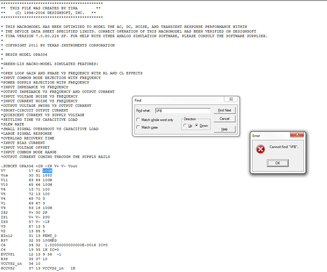
    This does not seem to be developed by us. The one of TI.com does not have the same construction and there is no VFB term as you can see below. Where did you find this model?

    From TI.com OPA336 product folder >> "Tools and Software" tab

  • I actually downloaded it from TI couple weeks ago.

    David
  • Hi David,

    I have downloaded the model from here: www.ti.com/.../toolssoftware. As you can see these models have not been updated since 2014. Can you send me the exact link where you got the model from. It will help us investigate further.

    Thanks for your patience while we work through this.
  • Actually I downloaded right from the TI web page for OPA336.

    However, this is not as important now. Please give me some advice on convergence issue with UCCx318-1 model?
    I tried different Integration Methods such as Trapezodial, Gear, Modified trap, different DC solvers, etc.

    Thanks.

    David
  • Hi Nikhil,

    I am testing all the sub circuits inside the unprotected model for UCCx318-1.  Can you tell me how the AMP3802 works?  What is VSS pin for?  Thanks.

    .SUBCKT AMP3802 20 8  3  21  SS
    *               +  - OUT GND VSS
    .PARAM ISINK=3m
    .PARAM ISOURCE=500u
    .PARAM VLOW=10m
    .PARAM POLE=200
    .PARAM GAIN=10k
    RIN 20 8 8MEG
    CP1 11 21 {1/(6.28*(GAIN/100U)*POLE)}
    E1 OUT 21 11 21 1
    Rfil2 OUT OUT1 100
    Cfil2 OUT1 0 318p
    Rfil3 OUT1 OUT2 50
    Cfil3 OUT2 0 100p
    R9 OUT2 2 5
    D14 2 13 DMOD
    IS 13 21 {ISINK/100} ; mA
    Q1 21 13 16 QPMOD
    ISRC 7 3 {ISOURCE}   ; uA
    D12 3 7 DMOD
    D15 21 11 DCLAMP
    G1 21 11 20 8 100U
    EB1 7 21 Value = { V(SS)-0.7 }
    V4 3 16 {VLOW-38MV}
    RP1 11 21 {GAIN/100U}
    .MODEL QPMOD PNP
    .MODEL DCLAMP D (RS=10 BV=10 IBV=0.01)
    .MODEL DMOD D (TT=1N CJO=10P)
    .ENDS

  • Hi David,

    We did not see a need to change the integration method. We usually change the DC and Transient voltage and current tolerances to avoid convergence issues. These are called different things in different simulators, but you can look for terms like RELTOL (if convergence is coming from both current and voltages), VNTOL (if convergence is due to voltage only) or ABSTOL (if convergence is due to current).

    Other options to try are the iteration limits. If you are getting a DC convergence error at time t=0, try increasing the equivalent of ITL1 in PSpice. For transient convergence errors, try increasing ITL4.

    Other options to try is to constrain the max time step. Something like 20ns would be a good option to try if the defaults do not work in your simulation.

    I hope that helps.
  • Hi David,

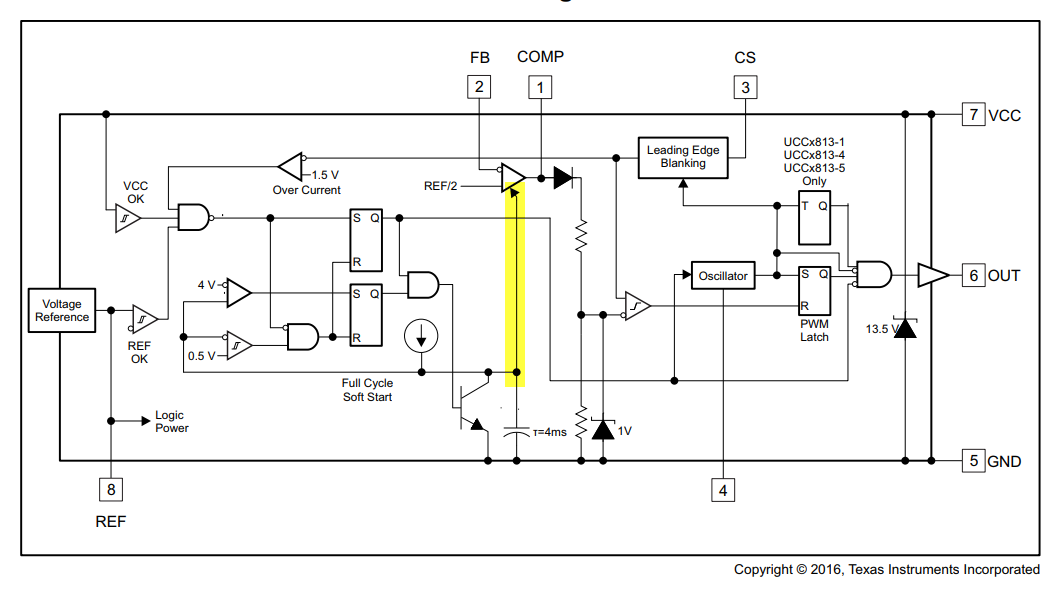
    The VSS pin or SS node corresponds to the node marked in Yellow in the block diagram below.

  • Thanks.

    About the convergence issue, does it help to set some Initial Conditions at nodes?

    About AMP3802, what is the best way to test it alone? I made an inverting amplifier with it and the gain didn't work. Please advise. Thanks.

    David
  • About the ss pin, what does it do? Does it enable the AMP?
  • The SS functionality of for the Soft Start feature. It controls the voltage the COMP is clamped to during soft start. You can find more information about this in the datasheet soft start section.

    Providing initial conditions may help with convergence but it may make it worse if the correct initial conditions are not provided. We do not use initial convergence to solve convergence issues, but rather to avoid the soft start if we want to test something in steady state directly. You can see an example of this in the TINA-TI Steady State reference design on the product folder.

    www.ti.com/.../toolssoftware
  • About AMP3802, what is the best way to test it alone?
  • You can apply a voltage on the SS pin and see of the output gets clamped and that the clamp voltage changes with the voltage on SS for fixed inputs. The inputs should be such that the output should be expected to be clamped.

    What is the purpose of testing AMP3802 separately?
  • Do I need to make an inverting amplifier (with output to inverting input feedback, and ground non-inverting input) first before the clamping test?

    I am trying to test every single sub circuit inside the UCCx813-1 model, then I will build a schematic of that, so that I can do more low level node testing to find out where my simulation problem is.
  • You can simply test it in open loop. Apply a large voltage on +ve input compared to -ve input (this will clamp the output) and see how the output (COMP equivalent) changes with the voltage on VSS (SS)
  • Yes, It works in open loop mode and clamp at 2.5V max. So this is not a real feedback type opamp model, right?
  • No, it is used in feedback mode in the actual device. SS pin is used during soft start. Once soft start is complete the COMP clamp volatge is fixed. Once in regulation (after soft start is complete), the external feedback and compensation network (which gets connected internally to this amplifier) will work to regulate the device when transients are applied.

    If you are testing SS functionality standalone, the compensation network should be irrelevant and you can test in open loop. If you need to test compensation, you will need to make sure that the SS voltage is such that the soft start is over. In the model this voltage is controlled by CTIMER which is clamped to VREF.

    Dtim ctimer vref _DCLAMP
  • Hi Nikhil,

    About the UCCx813-1 model issue I might have a break through. 

    In the sub-circuit below VON and VOFF have been defined two times.  What will be the final VON and VOFF?

    Also VT and VH seems to be non-standard VSWITCH parameters.  What are their functions?  Do they really work?

    **********************************************************************************************

    XUV VCC uvlout UVLOX2 PARAMS: VON=9.4 VOFF=7.4 ; UVLO Setting
    .SUBCKT UVLOX2  1   2  PARAMS: VON=4.1 VOFF=3.6
    *            VIN OUT
    S1 1 3 1 0 SUVLO
    RUV 3 0 100K
    EB1 4 0 Value= { IF ( V(3) > 3V , V(1) , 0 ) }
    RD 4 2 100
    CD 2 0 100P
    .MODEL SUVLO VSWITCH RON=1 ROFF=1E6 VT={((VON-VOFF)/2) + VOFF} VH={(VON-VOFF)/2}
    .ENDS

    *********************************************************************************************************************************************

  • Hi,

    Yes this is a standard hysteretic switch (acts as a schmitt trigger with turn on at VT+VH and turn off at VT-VH). It takes 4 parameters - Ron, Roff, Vt and Vh. Refer to this document page 161. There are also many other resources available on google that show the working of this switch.

    ti.tuwien.ac.at/.../scad3.pdf

    This is different from an exponential switch which does not have a sudden turn on. In this case the turn on/off is exponential in nature. This switch also takes 4 parameters but 2 of them are different from the schmitt trigger above) - Ron, Roff, Von, Voff. You can find the equations for this switch in this document on page 221.

    www.seas.upenn.edu/.../PSpice_ReferenceguideOrCAD.pdf

    In this particular case, VON and VOFF are just the parameters used to pass to the subcircuit. They are not the Von and Voff parameters that the exponential switch takes. The switch SUVLO depicted there is a hysteretic switch as described above. It is used for UVLO detection. Turn ON and Turn OFF points are defined by the value passed to the VON and VOFF parameters respectively (9.4V and 7.4V respectively in this case).