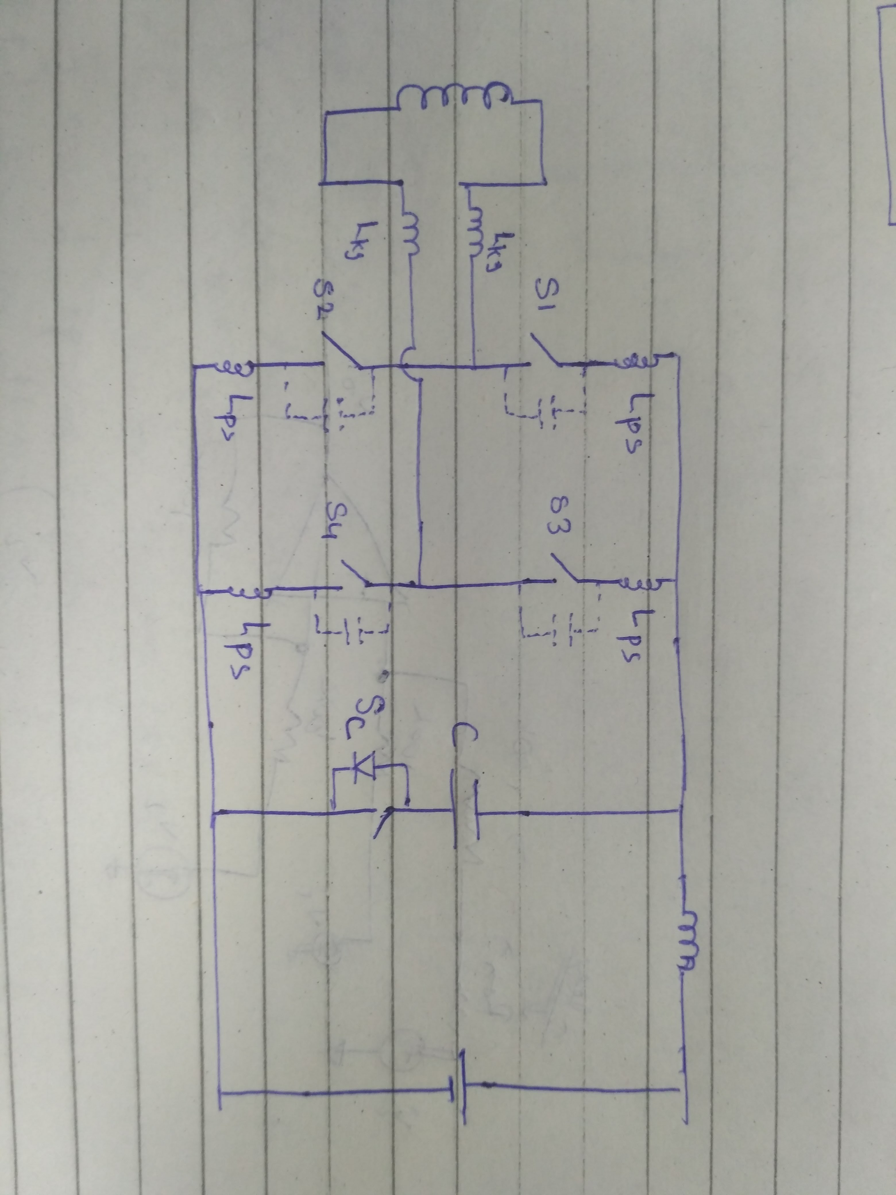
This thread has been locked.

If you have a related question, please click the "Ask a related question" button in the top right corner. The newly created question will be automatically linked to this question.

TIDA-00951: Snubber requirement for LV side Mosfets

Part Number: TIDA-00951


Hi,

While the converter is operating in buck mode (Charging mode) do we not require any snubbers for the mosfets on the LV side. Because the mosfet body diode reverse recovery current will cause a spike on the mosfet.

Also can you please briefly explain how the active clamp circuit is helping in reducing the spike and what exactly is causing this spike in the discharging mode.

  • Hi Eswar,

    I have answered this query in your other E2E post. I will add the reply here for the benefit of other users who might read your query.

    The di/dt of the current through the mosfet body diode is limited by the leakage inductor. Hence we don't see any significant reverse recovery on the LV mosfet.

    During discharge mode, the design works as a current-fed converter.
    In "traditional" current-fed converters (unlike voltage fed converters), there wont be any decoupling cap at the input of the switching power stage. Also the inductor current is continuous. As a result when a diagonal mosfet pair is turned off, due to the stray (mosfet lead, PCB trace) inductance there would be huge voltage spike on the mosfet.

    In this design the active clamp diverts the current out of the mosfet diagnol pair at turn-off hence elminates the voltage spike at turn off as the energy in the stray inductance will be very very low at turn off.

    Best Regards,
    Ram
  • Dear sir,

    Thanks for the reply.

    The active clamp operation during the discharging mode is still not clear for me.

    Consider the below pic :

    I have just drwan the current fed side of the converter with  parasitic inductances.

    During boost mode all the switches are turned on and the indcutor charges and discharges when one diagonal
    pair is turned off.

    Lets consider the switches 1 and 4 are off. Before turning off the Lps at these Mosfets are carrying current
    when the mosfets are turned off, the stored energy will be dumped into the Coss of the Mosfets which will
    result in spike.

    Now my doubt is how come the presence of the clamp circuit present at the boost inductor will snub the spike caused by
    parasitic inductance.

    I hope I expressed my doubt clearly.

    Thanks,

    Eswar

  • Hi Eswar,

    I have replied to this in your other thead fro the same question. Please check that for the answer.

    Best Regards,
    Ram