This thread has been locked.

If you have a related question, please click the "Ask a related question" button in the top right corner. The newly created question will be automatically linked to this question.

TIDA-00792: Charging issue with tida-00792

Part Number: TIDA-00792
Other Parts Discussed in Thread: BQ76200, BQ76940, BQSTUDIO

Hi,

I was evaluating TIDA-00792 for my personal project.

The board boots up fine, but i am facing a few issues.


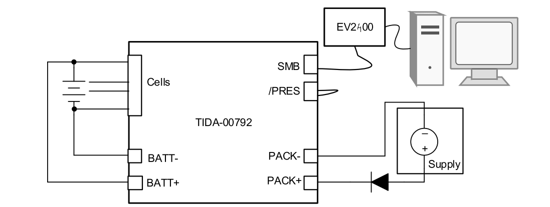
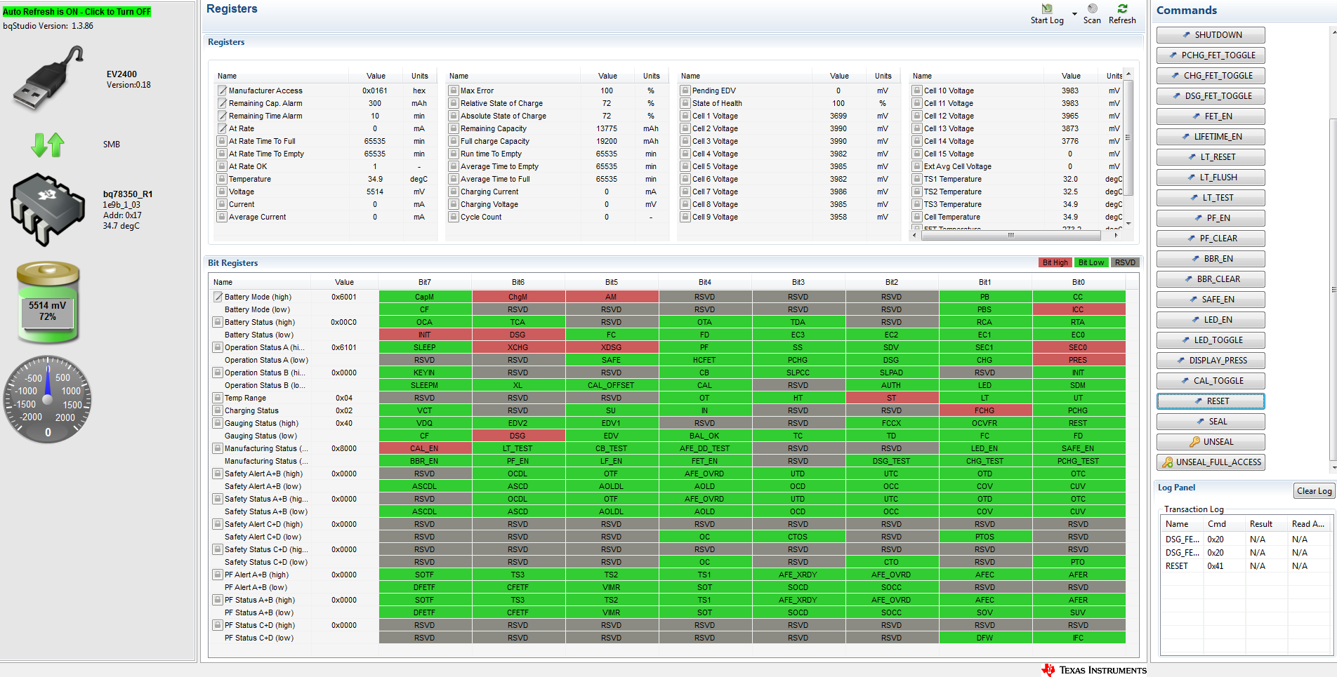
1. My setup looks like above and i am in the process of testing charging of my 14s8p pack made from NMC cells, the problem i am facing is as soon as i toggle chargefet, current rises but it stabilizes at 0.5 amp even though the supply is set at 10 amps CC. I have loaded the default settings and changed the following

Settings|Configuration|Temperature Enable 0F 

Settings|Configuration|DA Configuration 19

Settings|Configuration|AFE Cell Map 5FFF

Settings|Configuration|FET Options 0125

and i can't see any error flags being triggered. Please find the config file below.somewhat_working_low_current.gg.rar

2. The cell supports 3C discharge, so the maximum discharge current i can have is 57.6 amps, how do i configure this as the max limit is -32768 amps

3. Is there a tested configuration file for 14s 8p 2400mah cell that you guys can provide, it would be really great and highly accelerate my testing?

  • Hi Nakul,
    1. There is nothing in the design which should limit current. A BMS system is typcally designed to provide full current up to the configured threshold, then cut off and follow the supported recovery method. The issue is more likely circuit or equipment than configuration. You should look for the voltage drop with a meter or scope. Find the location that the voltage changes unexpectedly. With an 8P pack the cell voltage would not be expected to change much with charge current. If some protection is cycling it may have some PWM effect of apparently limiting the current and that should be easier or necessary to see with a scope.
    2. Scaling is the normal method to support high currents. You can manually scale if desired, 58A/2 would give a maximum data value of 29000, less than the 32767. Search on TI.com for the technique if desired. The bq78350-R2 firmware supports IP scale if you want to scale by 10. See the application note www.ti.com/.../slua726 table 2 for an example of the effects of IP scale. (there is an uncorrected error in the paragraph example, you will see it).
    3. Unfortunately there are not example files for different configurations.
  • Hi,

    I am still facing the same issue. I have attached logs of the voltages recorded across the board and the configuration file. Please help.

    recorded_voltages_and_config_files.rarAlso attaching my current config file:

  • Hi Nakul,
    In the gg file Settings Manufacturing Mfg Status init 0 hex
    shows that FETs are not enabled, and this looks consistent with the DSG and CHG voltages shown.
    In the voltages the DSG_EN and CHG_EN show 1.1 V? This would be on, but the DSG and CHG presumably from the bq76200 do not look on.
    In your setup you can turn on PACK+ without the load resistors, and this is a good way to start.
    Set the FET_EN bit in bqStudio. Be sure CHG and DSG from the bq76940 go high. Be sure CHG_EN and DSG_EN go high.
    Be sure CHG and DSG from the bq76200 go high and stay high, they should match the VDDCP voltage if inspected with a scope (10M or greater impedance). When they are about 10V above the battery voltage the system is on and you should be able to charge or discharge the battery. If there is a problem find and fix it.
    With the voltage be sure to follow any safety procedures for your facility and for your safety.
  • Hi,

    Please find the recorded voltages below.

    Here load is same three 10ohm/50watt resistors in series.

    Also R1 and R2 are shorted throughout, i don't know whether they can create any problem or not.

    WITHOUT LOAD (DISCHARGE) WITHOUT BATTERY (CHARGE) WITH LOAD (DISCHARGE) WITH (BATTERY CHARGE)
    1 TP7 - TP19 (BAT) 53.6 54.1 53.6 54.8
    2 TP4 - TP19 (PACK) 52.4 58.7 0 58.8
    3 TP7 - TP6 (VDDCP) 8.8 9.2 7.1 9.3
    PRECHARGE TP11 - TP19 (PCHG_EN) 1.6 1.7 1.7 1.6
    VPACK >14V , VBAT < VPACK, PACK(TP4) - PCHG(TP2) 11.1 12 41.4 12
    TP8 - TP9 (PGATE- PDRAIN) 0.9 1.1 13.6 8.4
    TP8 - TP14(2) (PGATE - CD) 13.5 1.6 13.6 8.4
    DISCHARGE TP12 - TP19 (DSG_EN) 12.7 0 12.7 0
    DSG_EN = HIGH , VBAT = VPACK , VDSG(TP3) - VPACK(TP4) 0 0.1 0 0.1
    TP15{1} (DGATE) - TP15{3}(PACK+) (Vgs) 0 0 0 0
    TP15{1} (DGATE) - TP15{2}(CD) (Vdg) 6.2 6.9 55.1 3.7
    CHARGE TP10 - TP19 (CHG_EN) 0.1 12.7 0.2 12.7
    CHG_EN = HIGH , VBAT = VPACK , VCHG(TP1) - VPACK(TP4) 1.2 3.6 54.2 3.6
    TP14{1} (DGATE) - TP14{3}(BAT+) (Vgs) 0 0 0 0
    TP14{1} (DGATE) - TP14{2}(CD) (Vdg) 7.5 4.5 0 0
    PACK MONITORING TP13 - TP19 (PMON_EN) 0 0 0 0
    TP4 - TP19 (PACK) 52.5 58.7 0 58.8
    TP5 - TP19 (PACKDIV) 0 0 0 0
    R105 (VCC - CP_EN) 0.6 0.7 0.6 2.4

    Is the problem with charge pump? If so, how did it work for TIDA-00792?

    Now neither charging nor discharging is working.

    Also attaching the status registers.

    Hoping for a swift reply.

  • Hi Nakul,
    See your picture above, notice the Operation Status A(low) register, the DSG and CHG bits are off showing DSG and CHG are disabled. This is because in the Manufacturing Status(low) register FET_EN is low. Refresh or scan the screen to be sure it is a current display. Enable FETs if needed using the "FET_EN" button in the commands pane on the right. The command is a toggle command, so click once then update the window. At present there are no faults shown in the safety alert or safety status, so the FETs should be free to turn on if enabled.

    R1 and R2 are an alternate connection of voltage sense signals and should be fine.

    In your voltages table above, each result column alternately shows voltage on CHG_EN and DSG_EN. One would think you have enabled FETs in some manner to get those voltages. More normally the FET_EN is set and the FETs are on unless there is some protection event, the battery is free to deliver or accept current. However you achieved the FET_EN, when you had that condition the corresponding CHG or DSG output from the bq76200 are not apparently on.
    Something is shorted, disconnected, the wrong value, installed with the wrong polarity, or damaged. Check with a local colleague if you don't find it.

    Check that CP_EN is high (2.4V).
    Check that VDDCP - BAT is high, ~ 10V. I would look at it with a 10M ohm scope probe
    Enable the FETs, or charge or discharge however you have done before. You could use the test commands.
    Confirm CHG_EN is high.
    Check the voltage on the CGATE, it should match the VDDCP. If not, find where the short is. If VDDCP drops to 9V it is likely hitting UVLO and turning off. See if the CGATE pulses as VDDCP rises and falls. Look at the voltages on both sides of R12. The charge pump can only produce about 40 uA, so voltage differences could be subtle.
    See the appnote www.ti.com/.../slua794 for waveforms if you are not already familiar with it.

    Do the same for the discharge path. There it is helpful if you connect BATT+ to PACK+ so the signals move less. From your measurements it seems you have done this in some cases.
    Obvious problems might be:
    D2, D3, and/or D4 installed backward or shorted
    R6 or R16 too small or shorted
    C2 missing or too small
    C5 too large ( but only for DSG, you have a CHG problem also)
    Poor VSS connection of bq76200
    L1-L4 missing or open, but probably not an issue with CHG or with BATT+ connected to PACK+.
    Shorted FET gate.

    The parts and the design work. You must measure and find the problem with the example you are testing. Manipulate the FET enables as needed to test, then set them on to operate.
  • HI WM5295,

    The issue was in the VDDCP capacitor. thanks for the help.

    Now i am facing another issue. I observed the balacing resistor r33 started getting extremely hot and bq76940 wasn't even in wake state. Soon when i turned it on the first 2 voltages turned to almost 0.

    So i observed there was a voltage drop of almost 0.31 V between C0 and BATT-.

    So i shorted R1 and it resolved the heating issue. 

    Now when i put the battery on a charge-discharge cycle, C0 misbehaves a lot, as in it's impedance is highest while discharging and charging which has brought down the usable energy of the pack.

    Recently i removed the r1 short and it started behaving normal again. It also wasn't heating up. 

    Today i removed the system and put it on another battery pack, i am again facing heating issues. 

    I don't understand what is happening.

    Please help.

  • Any update on this ??

    Please revert faster.

  • Still awaiting a reply.

  • Hi Nakul,
    R33 is the balance resistor for the bottom cell, cell 1.
    R1 is a resistor which gives an option to sense the bottom of cell 1 at the board rather than at the cell. This allows fewer wires or connections to the cell. The VC0 pin can't sense or really go much below GND. If C0 does go below GND (VSS) there will be a voltage across R69 which will turn on Q20 and R33 will get hot.
    It sounds like you have intermittant connection to the bottom of your cell, probably in the high current path (J1 to the bottom of the cell). When the connection is good you don't need R1. When the conneciton is poor you need R1 to carry the VSS current for the part and likely the battery current for the pack. When the connection is poor the circuit works but the part reports odd voltages for cell 1 (C0).