This thread has been locked.

If you have a related question, please click the "Ask a related question" button in the top right corner. The newly created question will be automatically linked to this question.

TINA/Spice/ISO1212: Low-side and high-side switches

Part Number: ISO1212
Other Parts Discussed in Thread: TINA-TI, , ISO1211

Tool/software: TINA-TI or Spice Models

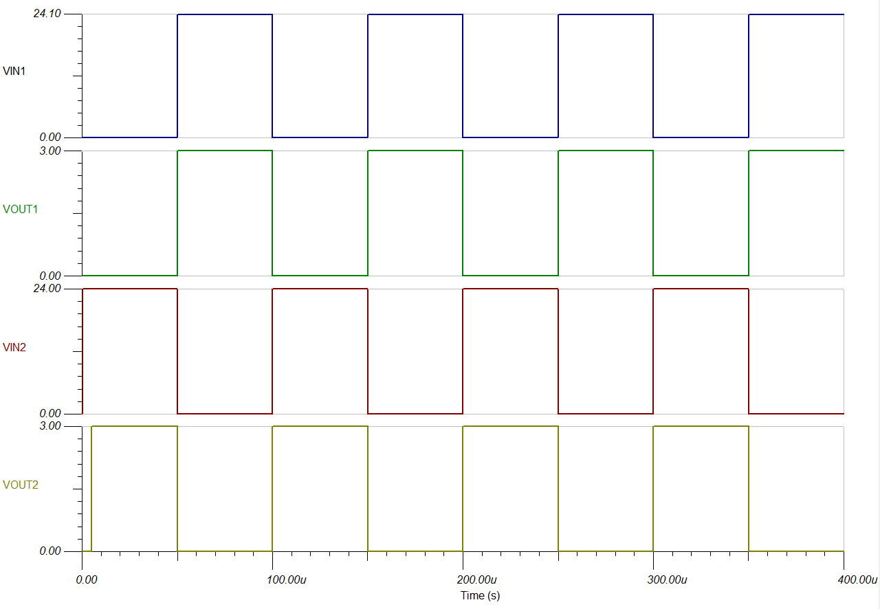
I am posting on behalf of someone in need of help with their ISO1212 simulation. The problem is as below.

I took sllm391.tsc, replaced the voltage generators with time-controlled switches and a 24 V voltage source wired one switch as high-side (switching the 24 V source), the other as low-side switch (switching GND). The high-side switch works, the low-side switch does not. I attached my circuit.sllm391_low_side.TSC

Respectfully,

Lucas Schulte

  • Hi Lucas,

    In the schematic provided, the low side switch does not work as the voltage at VIN2 will still be 24V(even if you switch it off). There is nothing blocking the source. Also, I could not understand your query completely, but from my limited understanding, I have modified the circuit slightly to get the below output. Please let me know if this is what you expected. If not, could you explain in brief what exactly you expect at the output.

    I have attached the modified schematic for your reference. 

    sllm391_low_side.TSC

    Regards,

    Karthik

  • Hi Karthik,

    Lucas was so nice to post this on my behalf, coming from this thread.

    In short: I want to replace an optocoupler input, which can be used in a high- or low-side configuration (either the switch is placed between the supply and the optocoupler, or between ground and the optocoupler).

    I tried to model that in simulation, because I was unsure about the placement of the Rthr resistor, and wanted to experiment with the placement. Actually, this is the circuit in "Figure 28. Typical Application Circuit With Sourcing Inputs" in the datasheet. But I couldn't get it to work.

    My original question was if the ISO121x simulation models are limited in this regard?

    What you did in your modified circuit was to revert my low-side configuration in the lower half back to the high-side configuration as in the upper part, which was already working.

    Regards

  • Hi Ronald,

    Thanks for explaining it clearly. Yes, there is a limitation in the model.

    The FGND pin is floating when the switch is OFF and PSPICE is calculating the FGND voltage value to satisfy the circuit. Because of this, the current model does not support the configuration specified. This has been added to the queue for a Bug fix.

    Regards,

    Karthik

  • Hi Karthik,

    thanks for clarifying this.

    Just out of curiosity, when this added to the bug fix queue, how long would it take until this is fixed? Would it be worth to wait for it?

    Regards

  • Hi Ronald,
    I will check with the internal team about this and let you know.

    Regards,
    Karthik
  • Hi Ronald,

    As mentioned by Karthik,we have debugged the FGND pin's behaviour for ISO1211 Model. Below is the same schematic that you tried for ISO1212 .

    Kindly let us know whether the below result is expected one and then we can modify the same for ISO1212.

     Regards,

    Ayan

  • Hi Ayan,

    this looks like the result I expected.

    Just as a remark: In my schematic the diode's anode was connected to the FGND pin, and not to the voltage source's GND, but I wouldn't expect any impact to the simulation result.

    Thanks a lot!

    Regards

  • Hi Ronald,

    Thanks a lot for your confirmation. We will modify the same in ISO1212 model.

    Regards,

    Ayan