This thread has been locked.

If you have a related question, please click the "Ask a related question" button in the top right corner. The newly created question will be automatically linked to this question.

WEBENCH® Tools/TIDA-00173: I customized the transformer of it

Part Number: TIDA-00173

Tool/software: WEBENCH® Design Tools

hello,

good day!

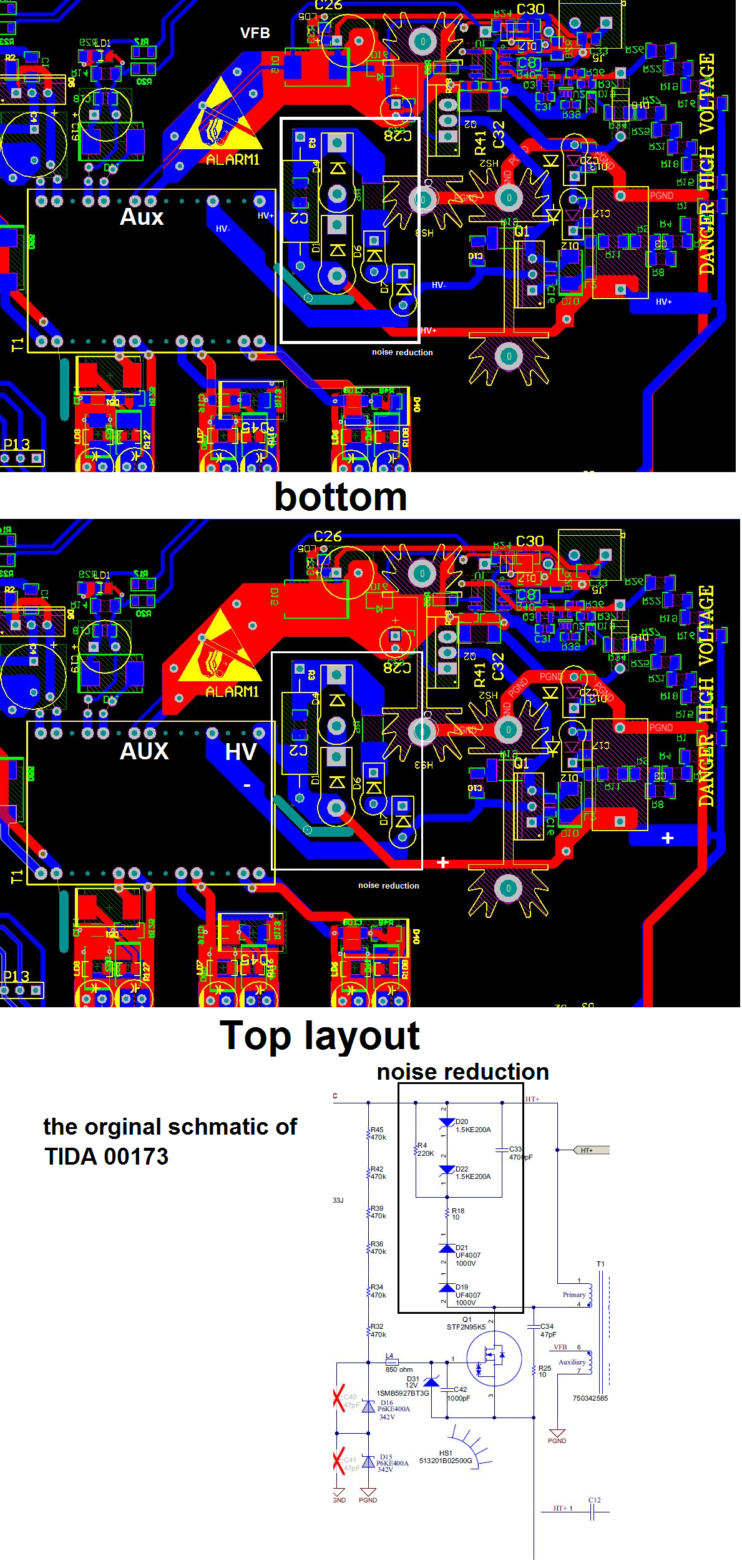
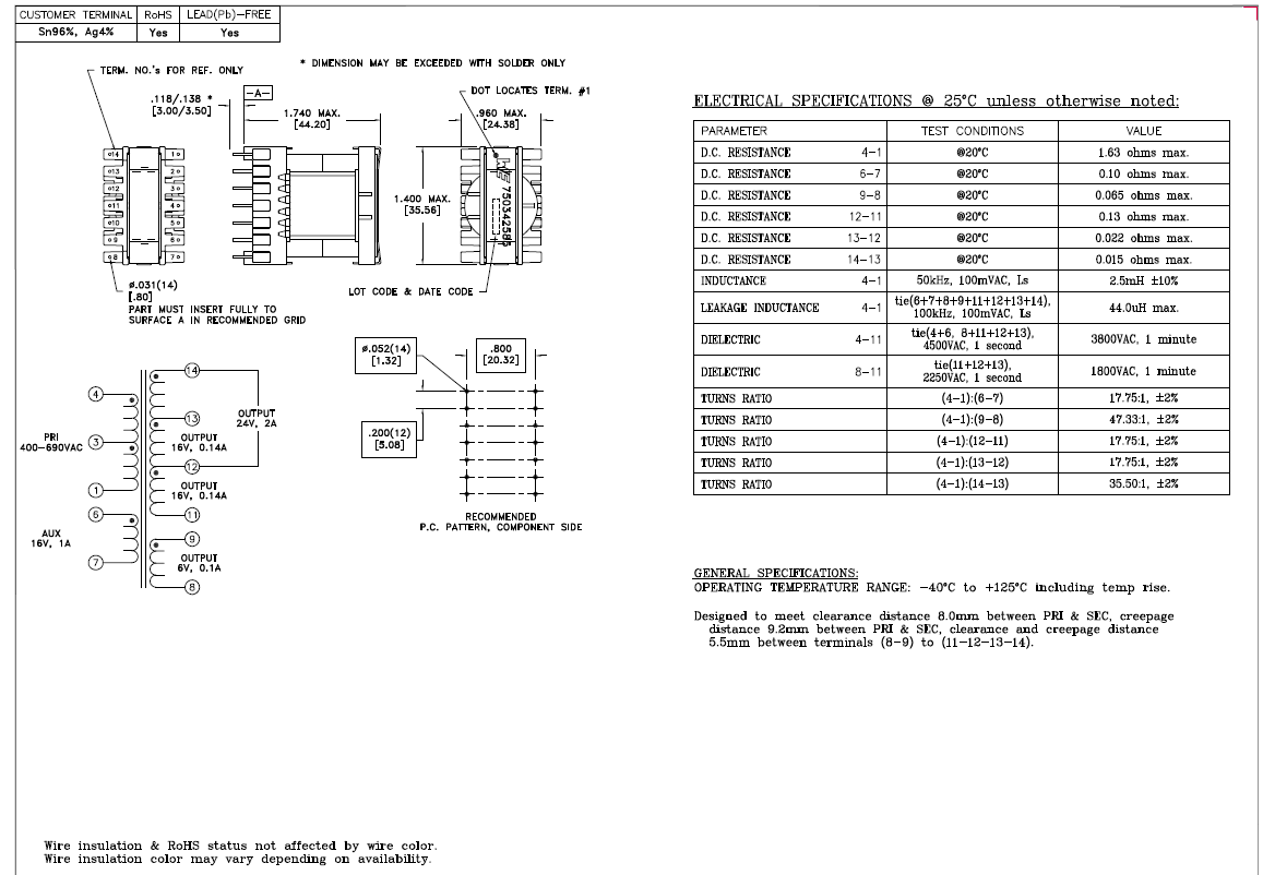
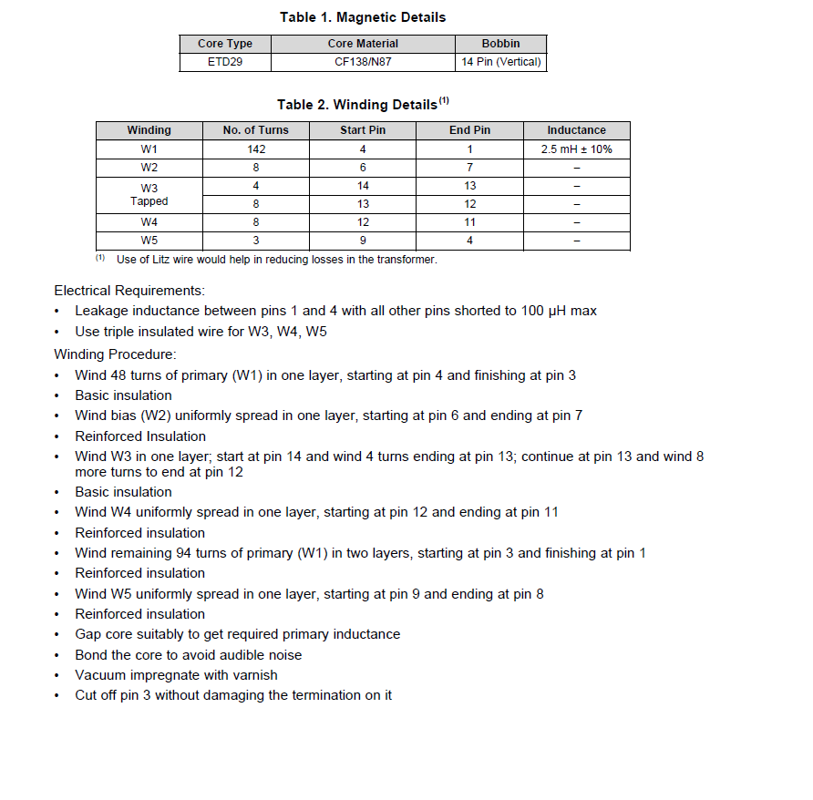
 I customized  the transformer of TIDA-00173 for my application to have :

    4 separate output for IGBT driver power 

1.GND_U VCC_U

2.GND_V VCC_V

3.GND_W VCC_W

4.GND_E VCC_E

one output for fan

5.GND_24 VCC_24

one  output for  function board 

6.GND_FNC VCC_FNC

one  out put for AUX ...

7.GND_AUX VCC_AUX

in put  voltage is 620VDC.

but sadly, It had very Spike in all of out puts.

so I came up with an idea to put capacitor (10nf 1000v) from HV+ coil pin to all of Ground pin in outputs (6 capacitor in total) .

in other word

C1(10nf 1000v) between  +HV ,GND_U

C2(10nf 1000v) between +HV ,GND_V

C3(10nf 1000v) between +HV ,GND_W

C4(10nf 1000v) between +HV ,GND_E

C5(10nf 1000v) between +HV ,GND_FNC

C6(10nf 1000v) between +HV ,GND_24

it works good ,and now my outputs have a small spike,

so,my question is that :

1. if is that wrong to put capacitor between primary coil and  all of secondary coils or not?

2.(as you know the IGBT driver powers must be separated from each other ),so those capacitor does have bad effect?

3.since it is customized transformer what else we can do to reduce the noise sound and spike of it.

thanks for attention .

Dave.

  • Dear Dave,

    thank you for using TIDA-00173. We will look into your questions with the designer and get back to you soon.

    Regards,
    Martin
  • Dear Dave,

    Thanks for reaching out regarding this query.

    I have a couple of questions to better understand the problem.

    1. Did you modify the transformer(and do other changes like adding 10nF capacitor) in Webench or some other simulation platform?
    2. If so, did you model parasitics(like inter winding capacitance) in the transformer?

    It would be great if you could share some waveforms, before and after adding the 10nF capacitor.

    Thanks
    Siva
  • dear siva
    I made it in real world not  simulation platform .

    perhaps I post my problem in wrong section.

    dave.

  • Dave, hello. You posted your question in the right place and we got the question to the right team here at TI. I saw your additional post on the same topic. No need for that one as the right team already is handling your question between Siva and Martin. We understand that you are working in real world per your reply. Any chance (as Siva was asking), that you might have some waveforms from your measurements before and after adding the 10nF cap?

    Best Regards,

    J. Fullilove
    Texas Instruments
    TI Designs
  • Hi Dave,

    No issues - this is the right section to post this. I wanted to have a clarification as to if this was observed in real-world or on a simulation platform.

    Please find the replies to the 3 questions in your initial query.

    1. if is that wrong to put capacitor between primary coil and  all of secondary coils or not?

    Ans. It is acceptable to put capacitor between primary coil and secondary coil - this is usually done to suppress common mode noise. Please ensure the capacitors are safety rated for appropriate voltage levels. Better to use Y-caps designed for this purpose.

    2.(as you know the IGBT driver powers must be separated from each other ),so those capacitor does have bad effect?

    Ans. No, as long as the capacitors are safety rated for appropriate voltage levels, there is no issue. The capacitors should be sized for suppressing the high frequency common mode noise and hence should not have any effect at gate switching frequency range.

    3.since it is customized transformer what else we can do to reduce the noise sound and spike of it.

    Ans. Improve the winding structure of the transformer to reduce the inter winding capacitance. It is this parasitic capacitance that conducts the common mode noise from primary to secondary and shows up as spikes on output voltage. 

    Hope this helps.

    Regards

    Siva

  • Thanks dear Siva I will send you my Altium Designer layout and also waveform of my power supply to help me more about that .
    because the switching transformer have very bad sound (noisy sound),I do not know if my PCB layout is my problem or the the switching transformer?...

    Regards
    Dave
  • Hi Dave,

    Please share the layout files of PCB and transformer winding structure.

    Thanks

    Siva

  • Thanks dear Sive for concerning about my problem here is my PCB layout but first of all I should mention that I lay out my PCB exactly as same as TIDA00173 the only change which I have made  is Noise reduction part which I signed in the pictures . but about the winding of transformer which you mentioned, I give it to factory to do that for me the winding turn in VH and Aux is according to instruction of    TIDA00173  datasheet but sadly they refuse to give me the structure of winding :(.

    perhaps the long track for Aux (VFB) or HV switching may cause a problem but in my board I did not have a choice to change the location of  transformer ..

    dear Siva may be that is the big request but ,would you please design a transformer.

    as you know the original form of transformer instruction is these two picture  

    so what I want is sort of like this one which I show in below ...

    I don't know how to design it .

    thanks for attention

    Dave. 


  • Dave,

    Thanks for sharing the layout information. The transformer PCB layout looks good except for the HV- track in the first image. HV- is the switching node and hence the source of maximum common mode noise. That track runs below the transformer winding region and increases coupling of common mode noise to secondary side. Please see if it possible t o re-route that track away from the winding region. Also, adding a shield layer(grounded) between primary and secondary winding helps in reducing the common mode noise on secondary side.

    Hope this helps.

    Thanks

    Siva