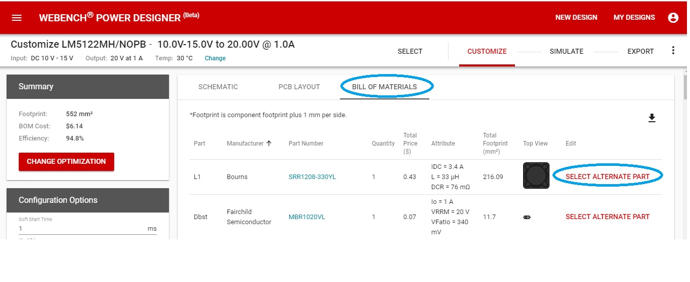
This thread has been locked.

If you have a related question, please click the "Ask a related question" button in the top right corner. The newly created question will be automatically linked to this question.

WEBENCH® Tools/LM5122: Eagle WEBENCH import pcb problem

Part Number: LM5122

Tool/software: WEBENCH® Design Tools

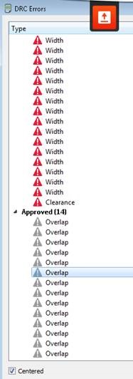
Hello I am having trouble importing the LM5122 configured using TI Power Designer. I am unable to export the schematic and board for Eagle 9.1.3 correctly. There are issues when running the script or opening the board/schematic files. 

Can someone help me import the file correctly?PCBEagle.zip

  • Hi Rajiv,

    I tried opening the LM5122 Schematic and PCB files shared above. 

    The issue might be because of the CUSTOM inductor in the design. Please select an Inductor with the nearest value from the 'alternate Inductor' list so that .SCH file and .BRD file opens without error.

    Please let us know if you have further queries.

    Thanks and Regards,

    S.Suganya

    Note: Please refer 'Read me' text document in the downloaded .ZIP files to import the Eagle SCH and BRD files.

  • Hi Suganya, Thank you for your help! Where can I find this alternate inductor list and how do I select this alternate inductor?
  • Hi Rajiv,

    Thanks for your reply. Please chose Alternate Inductor in any one of the following methods:

    a. From Schematic Page:

    • After choosing LM5122 in Power Designer, you will be directed to the Schematic page.
    • Click on 'L1' in the schematic and a window will open up which gives the description of the present inductor. There you can see 'Choose Alternate' option as shown in the image below.

    b. From Bill Of Materials page:

    • While you are in the Schematic page of LM5122 you can see 'Bill of Materials' tab. Please click on it
    • Scroll down to Inductor L1. There you can find 'Select Alternate Part' as shown in the image below. 

    C. In both the above methods the Alternate list of Inductor opens up where you can search/sort with your required Inductance values as shown below

    Thanks and Regards,

    S.Suganya

  • PCBEagle 3.zipHi Suganya,

    Thank you so much for the help. I have followed the instructions listed here and was able to obtain a schematic. However, when following the readme.txt instructions, the PCB board design is still not working. Could you help me with this? If not, how can I restart the design using the footprints in the current board file?

  • Specifically, I encounter many errors when executing the script to import the library.
  • Hi Rajiv,

    We are working on it. We will get back to you shortly.

    Thanks,

    S.Suganya

  • Hi Rajiv,

    The PCB has been designed for the default conditions provided in the WEBENCH considering the corresponding Bill of Material and quantity of the components.

    In the PCB shared(PCBEagle-3.zip) we observed COUT and COUTX are 4 in quantity and the footprint size is comparatively bigger. This is causing overlapping of the Cout and Coutx in the given PCB area. Please rearrange the components to avoid overlapping if this the design requirement. Or you can choose smaller size footprint for Cout and Coutx with reduced quantity.

    Please note: Choose resistor ‘Rt’ a different package which is 0603 or above which will solve the ratsnest issue in the PCB.

    Thanks and Regards,
    S.Suganya
  • Hi Suganya,

    Thank you for your help again. I followed your instructions and it fixed the errors you mentioned, but I am still running into errors with the board. After using ratsnest, I still find many errors in the board design. This design is becoming urgent since I am hoping webench export would be sufficient.

    Best regards,

    Rajiv 

     PCB-Eagle404.zip

  • Hi Rajiv,

    Sorry for my delayed reply. Below are the possible solutions to eliminate DRC errors generated in Eagle tool.

    Some of the Errors can be approved within the tool which will not impact the design or functionality of the design and other errors can follow the suggestions as stated below.

    1.    Overlap errors: Via on pads

    Via on pad is one of the methods for better connectivity of signals to the polygons. Vias on pads does not affect the functionality of the design. We understand that Eagle throws DRC message wherever it sees via on pads. There is an option in the Eagle tool to select these errors and make it as “Approved” DRC.

    2.       Drill Size Errors:

    The smallest drill size on the PCB file is 9mil which is the thermal via on the IC pad. This minimum value of drill size has to be set in the Design rules and the errors will get eliminated.

    3.    Air Wires (Unrouted nets) error:

    Eagle tool is Schematic driven and it always looks for consistency between schematic and PCB file. Since the SCH and PCB fie are generated separately during Exports, it does not recognize the netlist from the schematics. Currently, there is no option to combine them under a single project. However the exported PCB has all the connections/tracks routed. At present we don’t see any methods to eliminate the DRC related to Air Wires in the Eagle tool.

    Thanks and Regards,

    S.Suganya