Other Parts Discussed in Thread: TPS61021A
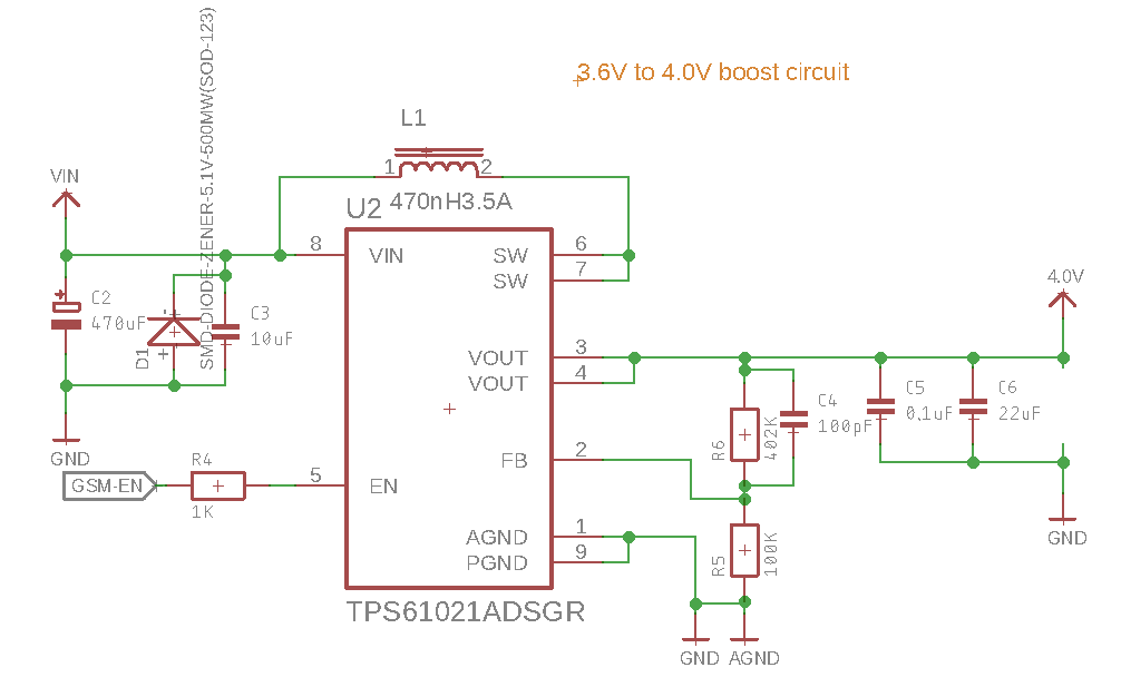
Can I use this zener diode: MMSZ4689T1 instead of the original one - 1SMB5918BT3G used in the design?
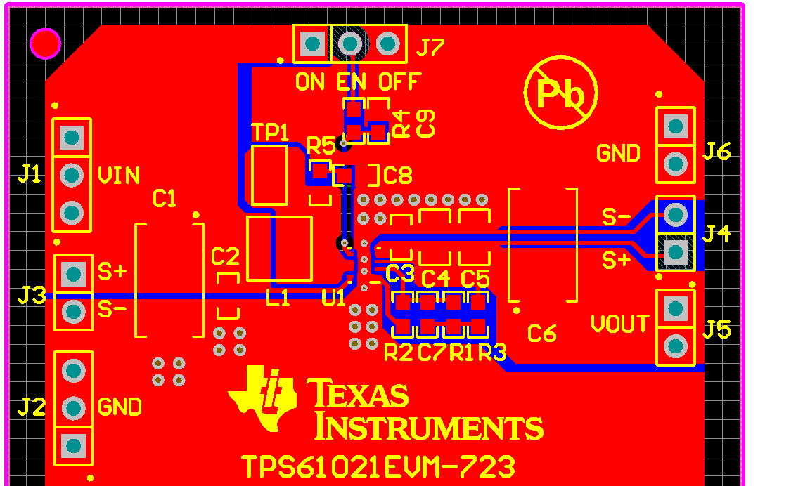
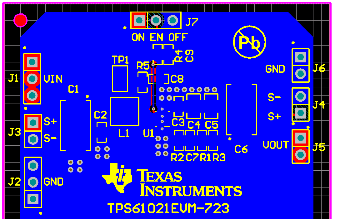
Also Ive created a gsm supply using reference design. Could you please review the layout and suggest improvements
if any?
Schematic:
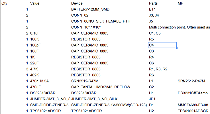
BOM:
Layout (VGSM trace is routed, though not visible below)