This thread has been locked.

If you have a related question, please click the "Ask a related question" button in the top right corner. The newly created question will be automatically linked to this question.

TIDA-01624: Currency of design files?

Part Number: TIDA-01624
Other Parts Discussed in Thread: TMP117

Hi there,

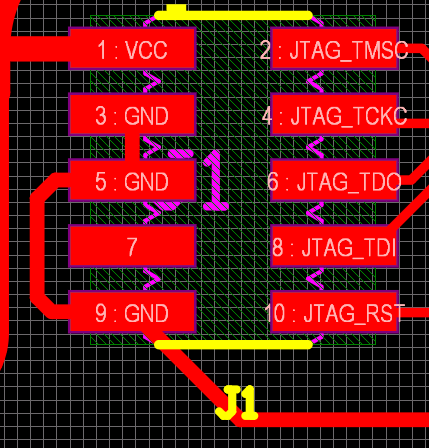
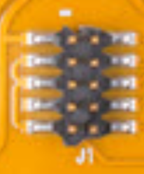
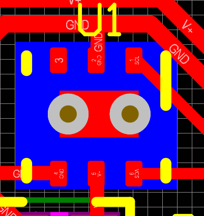
I'm looking at spinning off a few TIDA-01624s for evaluation.  The design files provided are Rev A, while the images shown in the graphics on the TIDA-01624 page are Rev E2.  Having a cursory review of the Gerbers against the tracks in the image, I did identify at least one difference.

Can someone from TI please explain the differences between the board revs and if necessary, provide the latest reference design files?  Thanks.

Cheers,
Zyrus

  • Hello Zyrus

    I do not think there is any difference between the uploaded Gerbers and the Image of the board. You can check that against the Altium database that is also provided in the Tool Page.
  • Hi Amit,

    There is indeed a difference.  See the trace between pins 3 and 5 on JTAG connector J1:

    Viewing the connector on the Rev E2 image shows the trace is routed around the outside, i.e.:

    If Rev A is fine, then no problem, I'd just like unequivocal confirmation.  , I saw your TIDA-01624 video on the TI page and you're also the schematic author - are you able to provide insight?

    Also, re. Note 1, "TOP COVERLAY OPENING FOR U1 SHALL BE 2.6MM x 2.6MM.. THERE SHOULD BE NO COVERLAY MATERIAL PRESENT IN THIS OPENING", noting the image below, presumably the traces running under the package to pins 1, 4, and 6 will be ENIG'd.

    If they are indeed exposed, my suspicion would be that during reflow, there is a risk that solder may creep along the trace and "bump" the package upwards slightly, potentially reducing heat transfer from the underside.  Would it make more sense to have the traces only entering from the pin-sides of the package?

    , note also that the Altium project provided contains only Rev A files.

    Thanks in advance for the assistance.

    Best regards,
    Zyrus

  • Hello Zyrus,

    First of all, the recommendation for the device is not to solder the thermal pad to avoid mechanical stress on the device. At the same time, the primary path of heat conduction is through the pads. Having a good contact between the thermal pad on the device and the PCB helps improve the thermal response.

    Secondly, regarding the change, I checked as well and yes, the change is an additional change done after reviews to make some of the traces a pass through instead of having a star connection. This would only improve reflections if any on the line and will not affect the design as such.
  • Hi Zyrus,

    Echoing what Amit Said:

    The change on those pins was done because it was observed it would make the ground connection slightly more direct. Rev A however is the most current version of the design files, and what I would recommend looking at.

    Regarding the traces under the TMP117, we didn't observe this problem during testing of the design, likely meaning that if it was occurring the effects were not significant enough to affect accuracy of the patch. You are definitely thinking along the correct lines for optimizing your thermal path though. Whether or not you've encountered this problem before, you should feel free to route the traces from the pin side if you would like.

    Best Regards,
    Brandon Fisher
  • Thanks and . I'll run with that!

    Cheers,
    Zyrus