A related question is a question created from another question. When the related question is created, it will be automatically linked to the original question.
If you have a related question, please click the "Ask a related question" button in the top right corner. The newly created question will be automatically linked to this question.
1. Yes, it is the channel switching frequency.
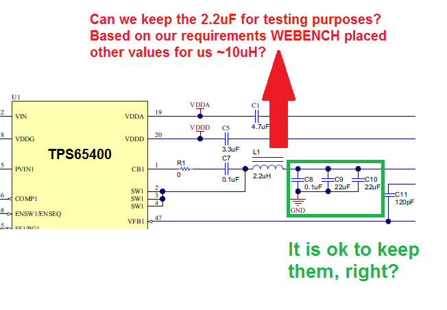
2. Cout value of 20uF is without the DC bias derating. If you check the derated value, it would probably be lower than 20uF which can lead to lower value on Ccomp or Cc.
3. Yes, really low values of Ccomp2 suggest you may not need it on the board though it is a good idea to check the actual measurements and ensure you have sufficient gain margin at higher frequencies so it rejects noise.
4. I see the power stage inductor and output capacitor are identical for all channels which is usually a big factor in how the compensation design works but not sure why all components are identical.
In addition to what I have said above, for questions 3 and 4, I am requesting a product expert to take a look and provide feedback.
Q3: The equation you get from datasheet is also an approximate calculation. What's behind the Webench is some mathematical equations and also bench validation results. I would suggest you to follow the Webench result. As the fF order result, you can just leave it open. Sometimes Webench does give out values which looks unreasonable. This is because the webench model always give out a non-zero vaule for each component on the schematic.
Q4: Compensation doesn't need to be very very accurate. The same compensation network can keep the loop stable for the default configurations on the EVM. However, as you required, Vout is much higher than the EVM (I remember it was 12V). This will need a re-design for the compensation.
A- Can WEBENCH simulate the TPS65400 in Current Sharing Operation?
If not, how can the calculation of Compensation components be done in the best way?
B- Can the EVAL BRD of the TPS65400 be used with Current Sharing Operation, I believe doing the HW edits it could work, but what about the when opening it with the PI-commander GUI? Any observations/recommendations?
C- One of our possible scenarios is having the output of one regulator of the TPS65400 as the VIN for other regulator of the TPS65400, that can be done right?
B. Yes, it can work in current sharing mode. CH1/2, CH3/4 can do the current sharing respectively. Please refer to the datasheet for detail. It seems that the GUI only support indicating the current sharing status... But doesn't support change the ISHARE bit in IOUT_MODE register(0xD6).
Do you need current sharing in your design? I remember the highest current is ~2A, single channel can support that.
C. Yes, you can do that.
D. For 1~3.3V, even 5V, you may keep the 2.2uH. For higher Vout, you do need higher indutance.
I have configured SW1 to provide 6.9V on its output, but when connect the output of SW2 to SW1,,,it drops like 0,5V
I have removed R7, R9 and C20,,,and I connected a jumper in J14 not only the voltage drops like 0.5V but when I load the SW1-SW2 regulators, a weird noise comes out, like a zzz, that is why I only measure the voltage and then I shutdown very quickly, I do not want to damage the device Is there anything missing to make it work in current sharing mode properly?
I also have a jumper in the EN2 in j8 of the EVAL BRD.
So based on what you are saying, I would need to change the ISHARE bit in IOUT_MODE register(0xD6) to make it work properly?
If this is the case, it does not make any sense you cannot do this with the EVAL BRD and the GUI, that means the EVAL-BRD -> GUI is not capable of reproducing all the features the device is capable off, however the GUI does detect that the SW1 and SW2 are now working as one, so it is pretty confusing for us, the users. Please correct me if I am wrong.
Our highest current nominal current is around 2A however in a worst case scenario there are peaks that could go up to 4A, so we were thinking on using SW1 and SW2 in current share mode (6.9V) also in case we would need higher current on that Rail, that is a possibilty we want to explore specially since the TPS65400 has the possibility of sharing the current. Then we would have SW3 with 5V and SW4 with 3.3V.
First of all, the max current demand is 4A right? Then why not put it on SW1 or SW2? TPS65400 currently capability is 4A/4A/2A/2A. Either of SW1 or SW2 can support 4A loading with single channel.
The GUI you are using doesn't support current sharing setting, it only have an current sharing indicator bit. There is another general GUI called Fusion, it's on the register level. You can have access to any register with Fusion. But it needs another USB connection tool, I'm afraid you don't have one...
As stated before, we might be needing more than 4A, that is why we want to use the current sharing.
1- I have the USB2ANY , wouldn't that work with Fusion?
2- WEBENCH has the capability of calculating the COMP circuit and the inductor for each regulator, how can I get the correct COMP circuit and inductor values, if for example I am using Current Sharing mode (SW1 & SW2) at 5A?
2. In current sharing mode as your example, feedback loop of SW2 will be disabled. Its PWM modulator will follow SW1. So for the COMP compensation, just consider SW1 itself. For the inductor selection, please keep SW2 the same with SW1.
So what you are saying is that if I use Current Sharing mode (SW1 & SW2) at 5A, 6A or 7A, and since WEBENCH will only let me simulate SW1 or SW2 at 4A, I should use the components for that current? Despite in this example I would be using more current.
For the current sharing configuration, I just think of there is a hardware method. You may refer to Chapter 8.3.6 on datasheet. Pull COMP2 or COMP4 up with 1k resistor, then it will be configured as current sharing mode.
1- If I use current sharing mode in SW1 and SW2 and let 's say I am going to use 5A between SW1 and SW2, to calculate the correct compensation circuit from SW1 and the inductors for SW1 an SW2, should I create a model in WEBENCH for 2.5A (assuming the current will split equally) or should I create a model of 4A (Maximum current for one regulator).
2- Can VIN (Analog VIN, PIN 22)be supplied by one of the outputs of the TPS65400 itself?
1. A design for 2.5A is good. Because in this condition, SW2 totally controlled by SW1.
2. Pin 20 is power supply for digital blocks inside the device. It's a output pin. Device has integrated internal regulator, and you only need to connect a capacitor on this pin. BTW, Pin 19, power supply for analog block, is the same.
Thanks for your reply, but you answered about pins 19 & 20. My questions is more focus about pin 22 (Analog Vin), which it is described in the datasheet as "Power input pin for VDDD, VDDA, and VGATE subregulator power".
Can pin 22 (Analog Vin) be supplied by one of the TPS65400 regulator outputs?
Sorry, I missed your point...
No, VIN can't be powered by any output of TPS65400. This power supply is for the device to work normally. No VIN, no output. VIN is the chicken, while output is the egg.