This thread has been locked.

If you have a related question, please click the "Ask a related question" button in the top right corner. The newly created question will be automatically linked to this question.

TIDA-060025: Amplifier design for Lidar

Part Number: TIDA-060025
Other Parts Discussed in Thread: TLV3501, OPA858, , TDC7201

Hi,

I'm part of an undergraduate design team that's working on a single beam lidar rangefinder system for our senior capstone.  We have been using your lidar reference designs for the 7200 and 7201 in our design thus far which have been very helpful.  We have decided that the 7201 should meet our needs due to the short time measurement mode.  We are trying to build a device that has a measurement range of ~10cm-10m.  There are some differences with our design vs the TI reference design (we are using an external visible wavelength laser diode and the PDA100A2 detector from Thorlabs).  It seems that the comparator in the reference design (TLV3501) needs 0.3V input for operation, however at the 10m distance we are getting about 25mV signal out of our detector.  No one on the team has extensive electronics design experience or has done any high speed amplifier design before, could you give any advice on how we could best add an amplification stage between our detector (which contains the photodiode and transimpedence amplifier)  and the comparator?  Any advice or tips regarding special concerns we should be thinking about would be great.  Also if you have any other helpful reference documents that we should look at.  Thanks!

  • Hello Sara,

        I am really glad that the TIDA-060025 reference design is helping with designing your application! I am assuming you are getting a 25mV signal out of the OPA858. Are you using the same or similar key system specifications as the TIDA-060025 reference design? Just to clarify, what is the bandwidth, rise and fall time, and supply voltage of your application? Also, what is the gain configuration of the transimpedance amplifier which I am guessing to be the OPA858 (correct me if I am wrong). I will be trying to find some reference documents, and post another reply to this post when I have compiled the list.

    Thank you!

    Sima 

  • Hi Sima,

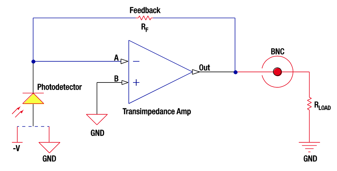
    There is a transimpedance amplifier in the detector (that we are getting the 25 mV out of on the oscilloscope).  I am not sure if it is the OPA858, the data sheet does no specify.  I attached the schematic of the detector if that helps.  We are trying to figure out if we need to add another transimpedance amplifier (or the OPA858 in a different configuration?) or if we are ok with just the comparator in the reference design before the TDC7201.  Or if there is a more suitable amplifier. I believe the other system specifications will be the same as the reference design.

    Thanks for your help!

    Sara

  • I would think we would need some kind of variable gain amplifier...since our detector output varies from the millivolt range up to several volts depending on distance to the target, and we would like accurate measurements within this range.  I'm so new to this kind of design, I am not too sure though.

    Thanks again,

    S

  • Hello Sara,

       Thank you for correcting me! I ended up looking up the PDA100A2, and it seems to me that it does indeed have a transimpedance amplifier which contains gain adjustment feature (by varying the feedback capacitor by a gain control knob). Were you and your team looking for more of an automatic gain control, rather than a manual one? Another option would be--like you mentioned-- using a variable gain controlled amplifier, which depending on the amplifier, could be controlled either by SPI interface, I2C interface or by an analog voltage.

         Back to the PDA100A2, which dB setting do you currently have the transimpedance amplifier adjusted to? It seems to have a gain bandwidth of around 600MHz and an output voltage of 0 to 10V (Hi-Z). If there is no need for automatic gain adjustment, the amplifier within the PDA100A2 should be adequate as an input to the comparator. However, you would have to take care not to exceed the common-mode input voltage range specified in the TLV3501 datasheet (V- - 0.2, V+ + 0.2V where V- and V+ are the power supplies connected to the comparator which the datasheet recommends a singly supply between V+ of 2.7V to 5.5V).

          Also, on the topic of TLV3501 common-mode input voltage range. After reading the TLV3501 datasheet, I was unable to locate where the comparator requires a input signal of 0.3V input for operation. Would you be able to pinpoint where this was understood?

          Just to summarize the above text if it is confusing:

              1. Will you be manually changing the gain depending on distance using the PDA100A2 gain adjustment knob

                        If yes, then there is no need for an additional amplifier 

                        If no, then you would need a high speed variable gain amplifier

    Would need to know bandwidth of signal necessary: Measure pulse width and I would also measure this at your min and max distance range using the oscilloscope to determine the necessary gain range limit

    Would be easier to implement if output voltage of the added amplifier does not exceed the input common mode range of the comparator (max 5.7V)   (Edit: Also TDC7201 has an input max of 3.6V which can not be violated)

      2. TLV3501 should work with a 25mV input signal. I was not able to locate where it would need a 300mV input signal. 

    Thank you!
    Sima 

  • Sima,

    I believe to simplify things we will just go with using the variable gain knob on the PDA100A2 and adjust depending on target distance.  We are building the lidar to use as an educational outreach device and it might actually make more sense for it to not be automatic as we could more easily explain what is happening as we manually vary gain.  At the maximum range of ~10 m during testing we needed to crank the gain up to the max 70 dB setting to register a signal, and down to lower settings as distance decreased.  We may still be able to get better performance from the detector by more precise alignment as well.  

    I think we misunderstood the datasheet when we were looking at the 0.3V value (this was listed in absolute max ratings, signal input terminal).  For future reference, does it specify anywhere in the datasheet what the absolute minimum voltage signal needed actually is?

    Thanks again!!

    Sara

  • "However, you would have to take care not to exceed the common-mode input voltage range specified in the TLV3501 datasheet (V- - 0.2, V+ + 0.2V where V- and V+ are the power supplies connected to the comparator which the datasheet recommends a singly supply between V+ of 2.7V to 5.5V)."

    Ok, I understand the different specifications in the datasheet better after reviewing some of the TI precision labs videos...Is there a better way to protect the circuit from exceeding this range, other than just being very careful with the manual gain adjustments?


    Thanks,

    Sara

  • Hello Sara,

       TI precision labs are an excellent resource for getting to know these products! Here's another resource that is very helpful with breaking down the meaning and use of each specification within any amplifier datasheet: http://www.ti.com/lit/an/sloa011/sloa011.pdf.

       Oh, I believe I see the confusion with the 0.3V value! For the voltage signal input terminal within the abs max ratings, you are correct with these specifications referring to the limits of the amplifier's input. However, the confusion would be in knowing V- and V+. These refer to the voltage supplies. Let's say you are using +5 V for V+ and ground for V-, then the input signal can not be any lower than 0 - 0.3 (-0.3V) or any higher than 5 + 0.3 V = 5.3V. This is why 25mV is not any issue in this case. The common-mode input voltage range is the range where normal operation of the amplifier is guaranteed, which in this case would be between: 0-0.2=-0.2V and 5-0.2V=4.8V; again, 25mV would not be an issue in this case either.

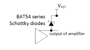
       There is a way to protect the circuit from exceeding this range which is through output clamping diodes. Here is an example at the output of the amplifier: 

       Vref would be at the power supply of the comparator between 2.7V to 5.5V. This protects the input of the cascading product (amplifer,ADC,comparator..) by placing the max output voltage at the referenced voltage + the forward voltage drop of the diode which for schottky diodes would be around 0.3 to 0.5V. Let's say V+ supply is 5V and V- supply is ground for the cascading product, then we would we need to place Vref at 5V for maximum output swing/input swing capabilities. Thus, the max output voltage would be around 5.5V as an input signal. Make sure this is an issue first by measuring at the minimum distance requirement the resulting max output voltage.

    Thank you,
    Sima

  • Sima,

    Awesome, thanks!  I understand it all much better now especially after reviewing more of the documentation.  We'll be sure to give you a shoutout in the acknowledgements section of our report.  :) 

    Sara

  • Hello Sara,

       I am glad I was able to help out! Feel free to open a new thread if you need further help or come up with any other questions!

    Thank you!
    Sima