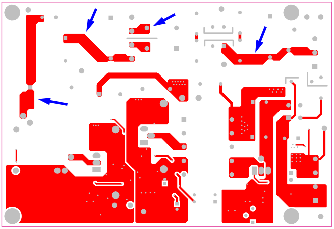
I have a question about the shape of the PCB traces in TI's reference design for the TIDA-00701 power supply. On the input/primary side, the traces are very chunky copper fills instead of linear traces directly between the pads. Is there an engineering reason for the shape of the traces? I recognize that necking down around certain pads is likely for thermal relief during soldering, but I'm trying to understand the reason for the oversized geometry elsewhere--the current capacity will be limited by the smallest cross section. Will there be any performance issues using straight linear traces? I've attached an annotated copy of one of the Gerber files showing the traces I'm referring to. Thank you for the help.