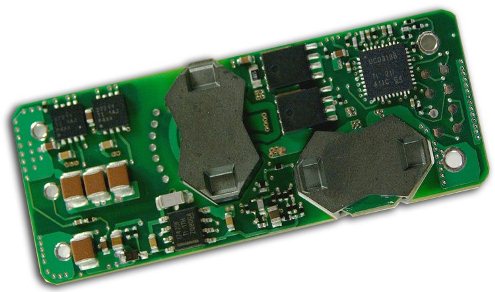
I was not able to locate any information indicating the layer stackup developed for this reference design. Would it be possible to access this information?
This thread has been locked.
If you have a related question, please click the "Ask a related question" button in the top right corner. The newly created question will be automatically linked to this question.
I was not able to locate any information indicating the layer stackup developed for this reference design. Would it be possible to access this information?
Scott, hello and good day.. Your query has been received and forwarded to our Power Design Systems team. The design owner and management team are currently on Holiday until the week of January 6th. You should receive a response to them the first 1-2 business days starting Monday, January 6th.
Best Regard and Happy Holidays,
John Fullilove
Reference Design Operations
Texas Instruments
I wanted to follow up and see if there has been any progress here. Thank you.
Hello Scott & John,
just checked it, it's a 12-layers PCB;
that's needed to provide the windings for the planar transformer solution.
Could provide a PDF prt of the PCB if that helps...
Best regards, Bernd
Thank you for getting back to me. Specifically, I was curious what dielectric thickness and copper weights were used. I have not designed any a integrated xfmr before and suspected the layer spacing may be important. Also, I was curious what copper weight was needed to handle the current in the power path.
Thank you,
Scott
Hello Scott,
unfortunately the responsible designer left TI some time ago.
I'm not able to figure out anything regarding the PCB itself.
Sorry for this & best regards, Bernd