This thread has been locked.

If you have a related question, please click the "Ask a related question" button in the top right corner. The newly created question will be automatically linked to this question.

TIDA-01505: Errors in the equations an few questions

Part Number: TIDA-01505
Other Parts Discussed in Thread: TLV431, TL431

So far, I found some mistakes in the application note:

  1. eq (35) R=(Vsn-Vtvs)/I=(450-330)/6.2=22R but Vsn is not 450V it is 360V
  2. eq (37) resalt is 103mA but it should be 103ms
  3. eq (38) resalt is not 314R but 314k.
  4. eq (40) result is 0.55W but it should be 3182W.
  5. eq (52) Mideal=((1/(3.14+0.5))/(1-0.825)=4.64 is not correct, it is 1.57
  6. eq (57) Measurement unit of Se is V//ms and what is measurement unit of constant 1 in the Se-1 part of the equation 57? Why Rramp and Rcsf are selected as 9k1 and 2k, respectively, when ratio between those resistors is 33.13 (Rcsf=Rramp/33.13)?

Few more questions:

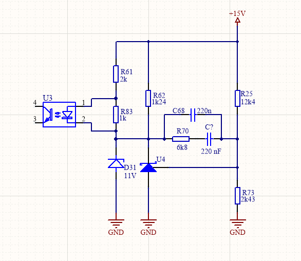
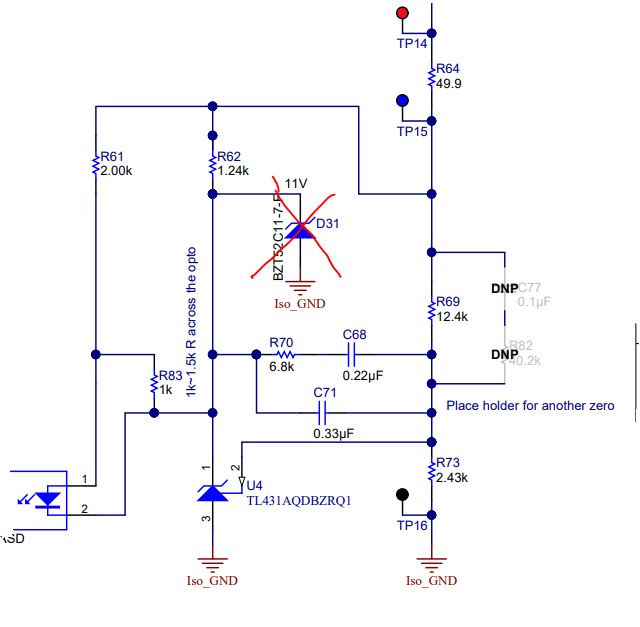
  1. What is the purpose of the zenner diode D31? The breakdown voltage of this zenner diode is 4V below U4.
  2. What is the purpose of the R74 and R75 and how to calculate them?
  3. What is the purpose of the R83?
  • Hi Kresimir,

    Thanks a lot for pointing out the errors. We will look into it and make the updates accordingly. Please see my answers below:

    D31 breakdown voltage is 11V which fix the voltage on the photo diode, the voltage change at the output will not be seen by the Vforward of the photo diode. The current into diode is fixed. This will the let the inner loop compensation be independent.

    The opto-coupler contains a parasitic pole that is difficult to characterize over frequency so the opto-coupler is set up with a pull-down resistor (R75) equal to 1 kΩ, which moves the parasitic opto-coupler pole further out and beyond the range of interest for this design. The R74 set the DC gain as 2.

    R83 provides the bias current into TLV431 for a high trans-conductance gain.

  • Hi Xun, 

    thanks for your help.
    I'm not sure where did the other questions from Kresimir disappear meanwhile, so please allow me to submit them again on his behalf:

    • Why is it necessary to introduce "blanking" time to CS pin with Q5?

    About Q9:

    1. Can it be replaced with SiC? Because it is difficult to find BJT with hfe>30 and 1700V Uce.
    2. Why should one use 2x1M resistors across C-E?
    3. For most traction inverters dV/dt=>20kV/us, so C36, C37 and optocoupler U3 seem not to be the best choice per Kresimir's comment. Can you comment?
    4. Application note says: Automotive 40V to 1kV, but most of the used components are not automotive qualified, including Q9. Are there any remarks on this?

    Thanks.

  • Hi Bart,

    Thanks for adding the questions here. Please see my answers in between the lines.

    • Why is it necessary to introduce "blanking" time to CS pin with Q5?

    It is not necessary to use it but it helps to blank out the spikes at rising edge as interference. When the spikes is not disturbing the IC operation the circuit could be removed.

    About Q9:

    1. Can it be replaced with SiC? Because it is difficult to find BJT with hfe>30 and 1700V Uce.

    Yes, SiC could be used with a Zenar diode placed between gate and source, but haven't tried yet. 

    1. Why should one use 2x1M resistors across C-E?

    This is not needed. Those resistors are the placeholder only when debugging the startup circuit.

    1. For most traction inverters dV/dt=>20kV/us, so C36, C37 and optocoupler U3 seem not to be the best choice per Kresimir's comment. Can you comment?

    This is correct. C36 and C37 could be reduced. They are just for EMI purpose. U3 could be replaced with optocoupler larger than 20kV/us.

    1. Application note says: Automotive 40V to 1kV, but most of the used components are not automotive qualified, including Q9. Are there any remarks on this?

    This is right. We mainly focused on selection of the IC device, and transformer due to limited time for development and resources. 

  • Hi Xun

    I really do not understand the point of D31 in parallel with U4. U4 is trimmed to be 15.25V, and D31 is 11V so U4 can be removed. What am I missing?

  • Hi Kresmir,

    Oh I see. Sorry this is a mistake. The D31 should be removed. It has no effect and should not be connected there. I was experimenting with it and forgot to remove from the schematic. I will get the schematic updated as well. Sorry for the confusion.

  • Hi Xun

    R69 and R73 will setup voltage the cathode of U4 to 15.25V NOT 11V! Why?

  • Hi Kresimir,

    When 11V Zener is placed, the R62 prevents the Vout being clamped to 11V.

  • Hi Xun,

    The purpose of R62 is obvious. I was asking why is voltage clamped to 15.25V with TL431 and when using zener diode then is clamped to 11V.  Probably both voltages need to be the same, 11V.

  • Hi Kresimir,

    Vout is always 15.25V, not influenced by Zener. It is set by TL431 plus the resistive divider of R69 and R73, which is: 2.5V*(R73+R69)/R73=15.25V

  • Hi Xun,

    Zener diode is parallel with TL431 so voltage will be clamped to lower zener voltage. 11V is lower than 15.25V so zener diode will conduct and TL431 will not. Of course, if zener diode is populated. If not, output voltage will be above 15V (15.25V+Vf(optocoupler LED)+V(R61)=19V)

  • Hi Kresimir,

    My understanding is that the R69 and R73 resistive divider is connected to the Vout, therefore Vout is regulated at 15.25V. Cathode of TL431A voltage is the Vout reduced by the bias current times pull up resistors, which is around 15.25V-Ibias*(R62//(R61+R83)).