A related question is a question created from another question. When the related question is created, it will be automatically linked to the original question.
If you have a related question, please click the "Ask a related question" button in the top right corner. The newly created question will be automatically linked to this question.
For a higher input voltage there will be increased stresses on the switching components. Thus D2 and D3 would need to be changed to 600V rated devices.
The VS resistors resistors help with start up and regulation. From section 7.1.3 you can determine the R3 value based on what minimum input voltage you want to start at, then R4 will be determined from the output voltage.
Do note that the 1:1 coupled inductor was used because the output voltage and the device's operating voltage are both 12V.
Let me know if you have any further questions on this
Is there any PSpice model for the IC "UCC28910" or a simulation tool for that?
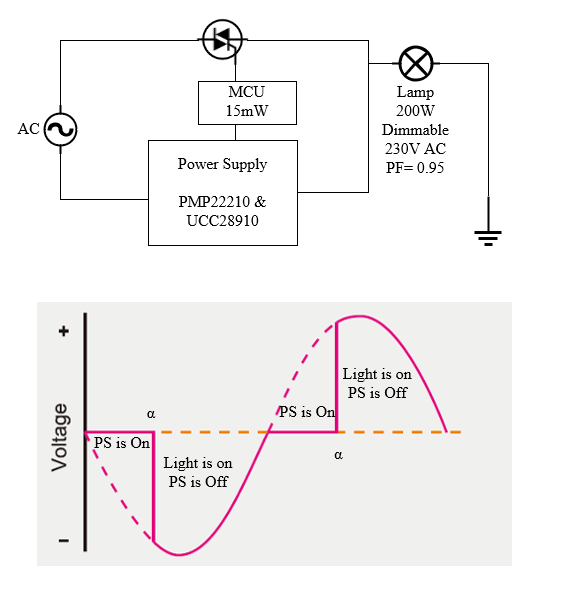
I need to evaluate the behavior of the power supply "PMP22210" while a Triac with the firing angle of Alfa in parallel with that is connected to an AC load of less than 200W.
1- if t<Alfa the power supply will work, and if t>Alfa, the power supply will be shorted therefore what will be the minimum of Alfa letting the power supply work properly?
2- In reference design documents I could not see clearly the transient behavior of power supply. I need to understand the behavior of the power supply in On-to-Off and Off-to-On states when the Triac will be switched.
I could not find a PSpice model on the product page.
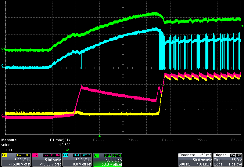
Below is a start up waveform for this design with a 120Vac input and a 20mA load on the output.From top to bottom: green is the bulk voltage, blue is the switch node, red is the VDD pin of the device and yellow is the output voltage.
In this waveform you can see the VDD charge up to VDDon, then because the Vbulk was not high enough switching was terminated. Later Vbulk was higher and thus switching was able to occur without crashing the bulk.
Can you clarify what behavior you are asking for? Is the source present? What is the load step that the Triac introduces?
Please consider a topology of Load+MCU+Power-Supply as shown in the figure. I need to know what should be the minimum value of Alfa (The firing angle of the Triac) so that the power supply has enough time to pass the transient state and reach the steady state then produce 12V DC on output.
It’s clear that at the very begging when all AC capacitors are discharged, the power supply to reach the steady state needs about 200ms as shown in your picture. But what should be the minimum of Alfa after (steady state condition of power supply) which prevents the high voltage capacitors to fully be discharged and also provides enough time for the power supply to quickly reaches its steady state condition.
Sorry for the delay. This would be correlated to the power factor of the supply at the different loading conditions.
Input Vrms
Output Voltage (V)
Output Current (mA)
Power Factor
230.1
11.99
10.000
0.263
230.1
11.99
15.000
0.279
230.1
11.98
20.010
0.296
230.2
12.00
25.010
0.311
230.1
12.02
30.010
0.296
For the specified 15 mW loading on the MCU you would expect a PF roughly 0.285. So for 50 Hz, that is 20 ms per period, 10 ms half cycle, them 0.285 * 10 ms is 2.85 ms.
This design was optimized for a large PF. The goal was to minimize the input rms current to as low as possible. If you need less PF then you would need to tweak the input filter.