This thread has been locked.

If you have a related question, please click the "Ask a related question" button in the top right corner. The newly created question will be automatically linked to this question.

TPS7A5401 - Output Noise issue

Other Parts Discussed in Thread: TPS7A54

Hi All,

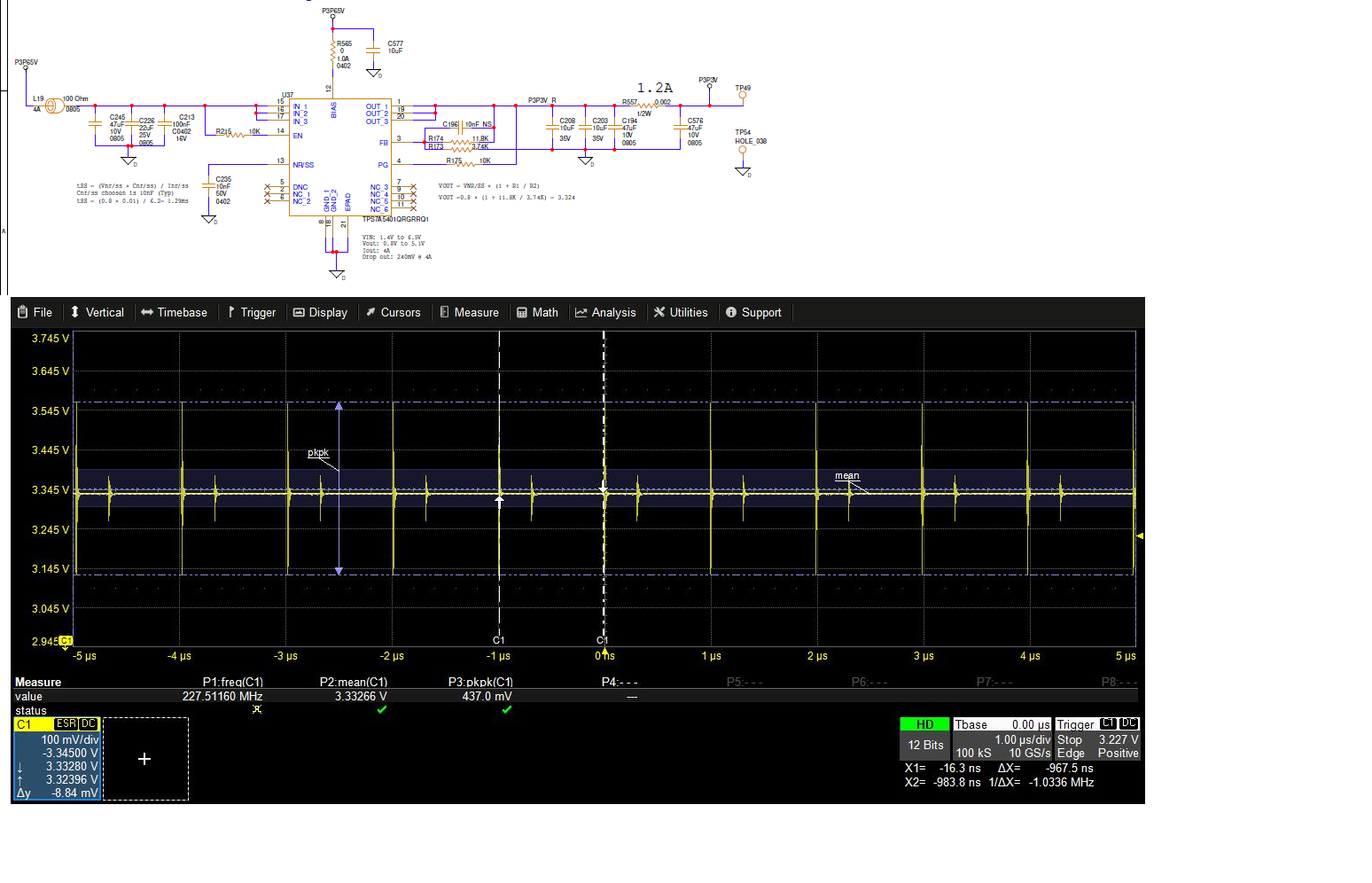
I am using TPS7A5401  to convert 3.65 Switching output to 3.3V. Switching regulator used is LTM4638EY#PBF and it has a noise of 20mV p-p at full BW. This noise is getting amplified by TI LDO TPS7A5401  and I am getting 450 mV p-p of noise at LDO output. It is causing all the reset and sensitive circuits to fail. I want help to get this noise filtered out. Circuit given below: Appreciate your help on this.
Regards

Prathapa

  • Hello Prathapa,

    The first thing you should do is to verify the layout does not allow the noise from the switcher to couple into the linear regulator.
    Please check that the return of the linear regulator is on the layer directly underneath the linear regulator.
    A return plane under the linear regulator will act as an electric field shield and prevent noise coupling into sensitive nodes.
    In particular, focus on the feedback pin, which is the most sensitive pin on the linear regulator.

    Please also check that the measurement setup supports a low noise measurement.
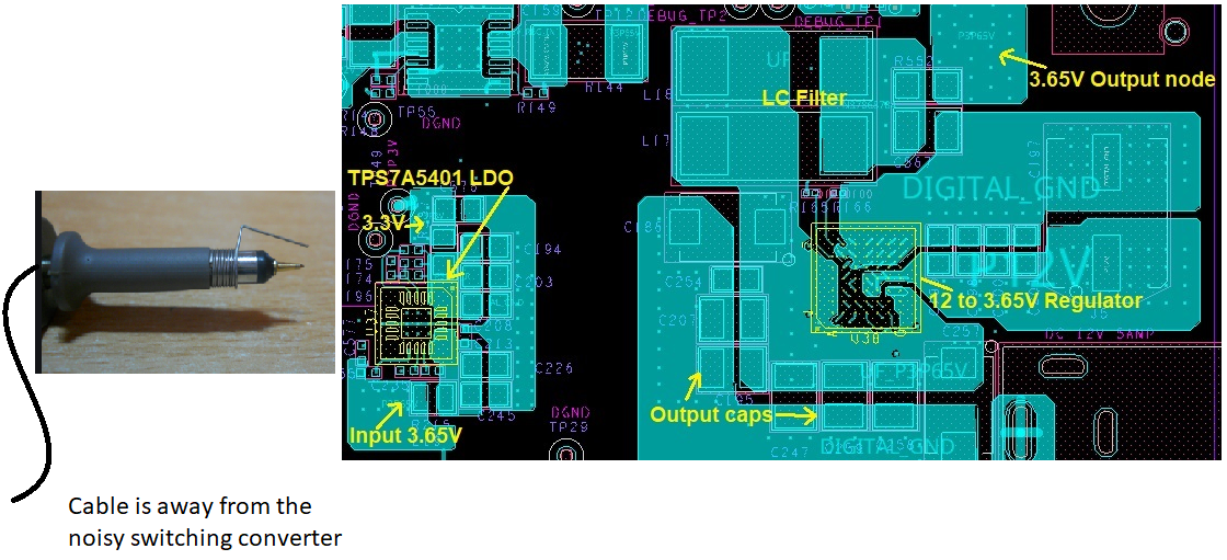
    The oscilloscope probes should not have long ground wires which can act as antenna's picking up the radiated emissions from the switching converter.
    The oscilloscope probes should be away from the switching converter.
    Using a ground coil around the oscilloscope probe will provide the best measurement.

    Thanks,

    - Stephen

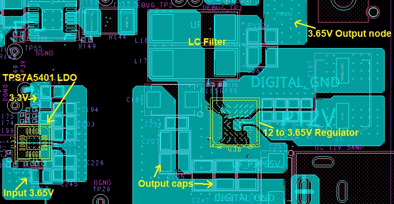
  • This is the component placement and the ground layer immediately below the LDO. We are also suspecting the noise being coupled from switcher regulator. Kindly suggest if there are any noise un-coupling techniques from the switcher circuit. Existing design have Ferrite bead at the input side and RC filter at output of LDO TPS7A5401. Below snap shot also shows the switcher regulator and LDO placement on actual board.

  • Hello Shrishail,

    Let's recap the sources of noise coupling to aid in our troubleshooting.  The are 4 types:

    1. Conducted noise using a shared impedance.  An example would be the output ripple of the switcher.  This ripple uses a trace or power plane to couple into the input of the linear regulator. This noise is what most engineers think of and a passive LC filter is often employed to reduce it. 

    2. Capacitively coupled noise (aka electric field coupling) - this is when large amplitude or fast ramp time dV/dt noise is present on the adjacent layer to a susceptible circuit.  An example would be the switch node on a high voltage or high bandwidth switching converter.  A common method to correct this is to use ground planes underneath circuitry to act as a shield, which you have here.

    3 & 4. Near field radiated emissions and far field radiated emissions. In our case the noisy power stage magnetic will emit electromagnetic noise, which can couple into measurements or electronics nearby.

    In your original statement you said the noise is being amplified, so that makes Conducted noise coupling unlikely, as a stable LDO cannot magnify the noise.
    One possibility is that the noise is coupling into the output of the LDO, and feeding back into the LDO through the Cff capacitor and into the feedback pin.  You can try remove the Cff capacitor and remeasuring the LDO output to see if the noise has improved.

    The noise looks to be at 1MHz, and the TPS7A54 should be giving you somewhere around 20dB of attenuation at this frequency.  Your layout has an electric field shield (ground plane) so this is also very unlikely.  This leads me to conclude that if the Cff removal does not improve the situation, the noise coupling is most likely through a near field emission, possibly from the power stage magnetic. 

    I would like to remove the measurement technique as the source of the noise coupling.  Can you take a measurement where the oscilloscope probe is entering the PCB from the side away from the switching converter?  And also using a ground coil.  See below.

    Thanks,

    - Stephen