This thread has been locked.

If you have a related question, please click the "Ask a related question" button in the top right corner. The newly created question will be automatically linked to this question.

PMP8740: PMP8740

Part Number: PMP8740
Other Parts Discussed in Thread: PMP, UCC28950, PMP6712, UCC29002, TMS320F28335, UCC28951, OPA378

Hi Roberto,

How are you? Hope you are back to office from vacation....

We have two PMP8740 boards ready and tested up to 2kW.  Before paralleling them, we want to try current sharing between the PMP8740 and LM5170EVM board. For the same, I need your inputs for the queries listed below:

1. Can we use a Schoktty diode (100V, 100A) at J18 pack pin 1, i.e before the load. The idea behind using  diode is to block the reverse leakage current when paralleling PMP8740 and LM5170EVM board. Can it be done? If so, should we change the compensation loop?

2. While sharing we want the PMP8740 board to operate in CC mode and also as a step by step process we want to start sharing starting from minimum  to maximum current rating of the individual boards (PMP8740 and LM5170EVM board). In such a case , is it sufficient to change R50, to set the Iref?

Please revert back at the earliest

Regards,

Anbarasan R

  • Hi Anbarasan,

    I am fine thanks: I hope you are doing well too! Vacation was great!

    You don't need to change the compensation, if you add a Schottky diode in series to the load, because when the diode conducts, it's actually a short circuit regarding the power stage transfer function.

    Also, for the second question, you are right: you can set a different reference for the current loop by changing the value of R50.

    In my design, Iref is modified by the PWM, provided by the microcontroller, as you already know.

    Best regards,

    Roberto

  • Hi Roberto,

    Current sharing between PMP8740 and LM5170EVM board is working fine. For a load of 2.5kW, PMP8740 shared 70% and LM5170EVM shared 30%.  Thanks for your inputs.

    Presently, we are using resistive load and we switch the loads in steps of app. 4A.  Can we increase the step to 10A. i.e we want to load the PMP8740 board in steps of 10A instead of 4A. Will it cause any issues?

    Regards,

    Anbarasan R

  • Hi Anbarasan,

    Thanks for your update: I am happy to see you are proceeding with testing.

    If you have a working current sharing circuit, you can increase the steps also up to 10A.

    Just, please, be sure during the load switching that there is no dangerous output current in each converter. For this purpose you should add a current probe on the output, and check during the transitions that there is no spike in both currents.

    Best regards,

    Roberto

  • Hi Roberto,

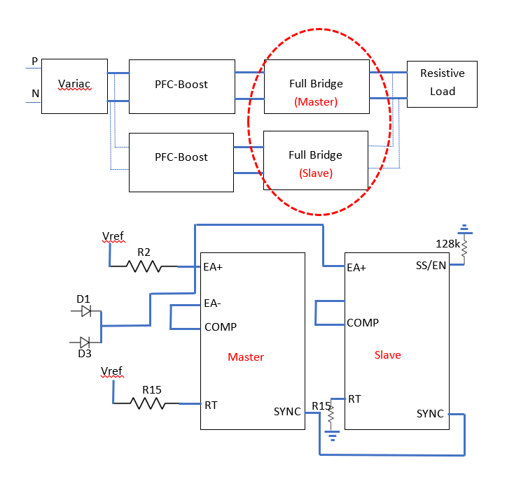
    I need your inputs for paralleling two PMP8740 board.

    Please find the attachment. Is it right? Please suggest...

    Should anything be done for the PFC controller?

    Please do revert back ASAP.

    Regards,

    Anbarasan R

  • Also, we have two desperate PMP boards.  Hence, we have to run small length wires to connect both the controllers-UCC28950. Will it make any issues?

  • Hi Anbarasan,

    The connection between one primary full bridge and one secondary full bridge you showed looks correct.

    From my point of view, this type of connection works well only if the two controllers are placed on the same board, or the distance between the controllers is also small (millimeters). If you have the controllers placed at tens of centimeters distance, I am afraid the signals can be corrupted by noise.

    Here is a link to an example, of paralleling two UCC28950, but taking place on the same board, see PMP6712 schematic:

    The whole documentation is available at the link:

    Since in your case you have two separated boards, I suggest to run them separately, with two voltage loops, to be balanced by using the paralleling technique explained in the UCC29002 (load share controller) datasheet, or using the digital parallel I employed in my PMP8740.

    Regarding the PFC boosts, there is no need to make any current or power sharing, since they are connected to mains, which has very low impedance.

    Please let me know if you have further questions.

    Best regards,

    Roberto

  • Hi Roberto,

    Thanks for the docs. It will help a lot...

    We are running out of time, and not really in a position to try anything new i.e using a separate load share controller nor using digital technique.

    We have best soldering experts, and we plan to mount the boards as close as possible.

    Attached-is the rough mounting of the 2 boards.

    We estimated a total wire length of app.10cm between the two SYN pins.

    Is it worth trying? Please suggest

    Regards,

    Anbarasan R

  • Hi Anbarasan,

    The boards look pretty close to each other, so it might work.

    In order to minimize any noise, captured by the wires, please provide some filtering (from example from the COMP output of the main converter, to the input of the second one, by using a RC filter (keep the filter on the secondary controller as close as possible to the IC).

    Regarding the oscillator and synchronization, please check that the signal doesn't corrupt while transferring from one board to the other.

    Regards,

    Roberto

  • Hi,

    Sorry for troubling you.. I couldn't get you...

    We connected EA+ of the main converter to EA+ of the slave converter removing D1 and D3 of the slave controller. EA- and COMP pin are shorted in both the master and slave.

    So, where should we need a filter; at the COMP pin or at the EA+ pin.

    Regards,

    Anbarasan R

  • Hi Anbarasan,

    No need to sorry! :-)

    I didn't know that you removed the two diodes.

    I suggest to follow the schematic of the PMP6712 that I already sent the link. If you referrer to this schematic, the output of the error amplifier is available on R30 (net OPTO-E), then there is the internal error amplifier with gain = 1 (R31/R32), where the reference voltage is on EA+ of U5 (half of REF1).

    The output of the primary (main) converter is now the net COMP1 (which is used by U5 to close the loop).

    The information of COMP1 is now sent to the secondary full bridge controller (see U11), which enters in the pin EA+. As you can see here, there is already a series resistor R74, so you need only to put a capacitor between pin 2 of U11 and ground, let's say 470pF (which together with 10KOhm resistor R74 makes a filter at ~ 32KHz). After that, R75 connects EA- with COMP of the secondary converter (with a gain of 1).

    This should be sufficient to have a primary/secondary architecture.

    If you are still unsure how to connect the primary controller, please send me a bigger section of the schematic you are using.

    Regards,

    Roberto

  • Hi,

    Am still confused.

    In PMP6712, the output of the error amplifier (OPTO-E) is given to EA- and COMP pin. EA+ is fed with half of REF1.

    In PMP8740 design the output of U1A and U1B is given to EA+ through diodes D1 and D3. We are following the same architecture for the master controller and for the slave we removed the diodes D1 and D3, connecting its EA+ from the master controller i.e EA+ of the master and slave are shorted. Hope am making it clear. Can we use the same?

    If we need to use the PMP6712 architecture, we should interchange the pins right. i.e the output of U1A and U1B should go to EA-  and COMP pin while EA+ should be given fixed reference. Why cant we use the PMP8740 method itself?

    Regards,

    Anbarasan R

  • Attached-rough schematic;

    Hope this is fine.

  • Hi Anbarasan,

    You are right! This last connection works. The point here is to avoid that the connection between pin EA+ of both controllers does not take noise.

    For this purpose, it should be sufficient to connect a local capacitor (220pF...470pF) in each controller from EA+ and local ground. In order to decoupled these two capacitors, you might add a small resistor (100 Ohm) in series to each connection to the two diodes D1 and D3, which shouldn't be removed.

    I created and attached a schematic only for the controller sections. The filter capacitors and resistors are Rf1, Rf2 and Cf1, 2Cf.

    Best regards,

    Roberto 

    PMP8740 2KW Rev_E Full Bridge - parallel.pdf

  • Hi Roberto,

    Thanks for the schematic.

    But earlier this morning we did the paralleling and the secondary MOSFET of the slave unit failed, when we increased the voltage above 50 volts.

    Please find the attachment-schematic which had failed.

    I have highlighted the changes in the RED circle. This time we connected COMP pin of the MASTER to EA+ of the slave. What would have caused a failure in the above case?

    Also, can we try disabling the secondary MOSFET permanently.  Will the body diode withstand the rated current? Most of the time the failure seems to happen in the secondary MOSFET.

    Please revert back ASAP

    Regards,

    Anbarasan R

  • Hi Anbarasan,

    The connection regarding the parallel is also fine. I would recommend to remove the resistor R2 in the secondary controller, since it makes no function.

    I am afraid you get noise into the SYNC pin of each controller, so it will be difficult to make it working without having both controllers on the same board.

    Regarding the sync-FETs, the losses in the body diodes at mid to full load will be too high and can lead to failure. You may test the converters up to 10%...20% of nominal load, unless you replace the sync-FETs with Schottky diodes, then, with appropriate heatsink, you may reach full load.

    Best regards,

    Roberto

  • Hi Roberto,

    Thanks for your inputs.

    Without using  serial communication (UART) can we do paralleling. i.e using a external controller (TMS320F28335)  but not using serial communication.  If so, how can we implement it.

    Regards,

    Anbarasan R

  • Hi Anbarasan,

    It is possible to parallel converters by using C2000 series (like the F28335) without the need of serial communication (UART).

    In order to do that, you have to sense and read the two output currents (best is to sense both inductor currents) in real time.

    Since it concerns software, and I am actually an analog engineer, you can post this request into C2000 threads.

    Best regards,

    Roberto

  • Hi Roberto,

    1) We tried paralleling today as per your suggestions. Filters were added to the EA+ pins of the master and the slave. We loaded the converter up to 6A.  The sharing was unequal i.e Slave 3.75 and Master 2.25. What could be the reason for the difference. The difference seems to increase with load? 

    2) Does the filter change the compensation of the loop, which is what creating a difference in sharing? Can we remove the filter and check?

    3) Please suggest what should be do to the SS/EN pins of Master and slave. PMP8740 design is different from SLUSA16D. As of now, we used 825k resistor and grounded the SS pin of the slave. Master remains same as PMP8740

    4)Instead of connecting the EA+ of Master to EA+ of the slave. Can we connect COMP in of Master to EA+ pin of the slave. In such a case shall we remove the C79 (connected between COMP and ground) in PMP8740. 

    Please revert back at the earliest.

    Regards,

    Anbarasan R

  • Hi Anbarasan,

    Here are my answers to your points:

    1) At low output current, it's normal that there is some unbalance: this is due to the difference of the peak ripple inductor current of each DC/DC stage, plus small difference in the internal blocks of the UCC28951.

    2) No, the filter is not impacting the loop compensation as long as the pole, introduced by the filter, is far away from the crossover frequency (for example the pole frequency is 5...10 times the Fco).

    3) In the main converter the soft start pin should be connected according to the PMP8740 design, while for the secondary converter it can be connected to a small capacitor to ground (1...10nF) and left it alone, because the secondary converter is controlled by the main one also during soft start.

    4) Yes, this is also correct. BTW, you can leave a small 100pF capacitor here, to avoid some noise.

    Best regards,

    Roberto

  • Hi,

    Thanks for your inputs. Will try to know tomorrow after testing

  • Hi Roberto,

    We tested sharing up to 35A today- Slave 18.5A and Master 17.71A. For this, we were using a single 1 PFC board + 2 DC-DC converter board.

    When we tried with sharing with 2 PFC board + 2 DC-DC board, the output voltage of the PFC board is oscillating from (380-384V) for a load current of 6A. What could be the issue? Actually , when the PFC boards were tested individually, there were differences in the output voltage- one settles at 389V and the other at 384V. Is that the reason for the oscillation? Should be regulate both to equal voltage or should we change anything on the PFC board?

    Regards,

    Anbarasan R

  • Hi Anbarasan,

    I think the performance of the current sharing is good, because it's within +/-2% (here the average output current is 18.1A).

    The output voltage of each PFC should not impact the regulation of the respective DC/DC stage, so it sounds strange to me that you have oscillation on the PFC stages.

    Of course you are not connecting the outputs of the PFC stages together, correct? If so, it could lead to oscillation and even fail of this stage.

    The only reason I can imagine the PFC is varying, is that the DC/DC is also supplying oscillating output current; in this regard, please double check it by analyzing the output current of the PFC with a current probe, attached to the scope.

    Regards,

    Roberto

  • Hi,

    We are not connecting the PFC stages together.

    As of now, we use 2 separate power supply-12V for the DC/DC stage, and the grounds of them are tied together. This that a issue.

    Regards,

    Anbarasan R

  • Hi Anbarasan,

    I think I understood why the parallel of your two DC/DC converters is having some issues. The origin can be the connection between the two grounds.

    I prepared a sketch, showing the secondary side connection of two DC/DC converters (named "1" as the primary or main, and "2" as secondary), see attached file:

    PMP8740 PSFB - Ground connections to avoid.pdf

    As you can see, you are connecting together GND1 with GND2 with the wire "A". But when you conenect two DC/DC converter in parallel on the output, you do that by tying both pin 1 and 3 of J8, with the wires "B" and "C". 

    As you can see, the wire "B" and the wire "A" are shorting both current sense resistors R91-1 and R92-2. 

    In theory you should have no signal on these resistors and collect no output on Iout-1 nor Iout-2. Probably you get still these outputs because the resistance of the connections "A" and "B" is comparable or higher than the value of each resistor R92-1 and R92-2.

    That means, you should avoid the connection "A", but, of course, this is not possible, because you need both controllers UCC28950 sharing the COMP signal, and therefore having a single ground (otherwise the CMOP signal would be not usable).

    In my architecture, when I connect together several modules of PMP8740, I use the connections "B" and "C" but I do not connect the grounds GND-x together.

    The PMP8740 is designed to have all GND-x connected by means of resistors (see R123 and C98 on page 3 of the schematic). This way, regarding the signal on the current sense resistor, there is no short circuit between modules.

    Let's go back to your case: here, in order to be able to connect also all GND-x (wire "A"), I suggest to move the current sense resistor R92 on the positive output (pin 1 of J8). If you do that, you may want to replace the operational amplifier connected to R92 with a high-side current-sense precision amplifier, from the INAxxx series. Please let me know if you agree.

    Best regards,

    Roberto

  • Hi Roberto,

    Thanks for your inputs. Will go through it and get back to you shortly.

    We tested sharing up to 55A today- Slave 29.6 A and Master 25.5A. The difference increased a bit higher, but we were able to share 2 PFC and 2 DC/DC converter boards together.  The output voltage is also stable at 52V.

    We are planning up to increase up-to 70A tomorrow. Hope it works.

    Regards,

    Anbarasan R

  • Hi Roberto,

    We tested the board up to 68A today: Master 33.2A and slave 34.68A ... We almost reached the full load capacity of individual boards. Thanks for your support throughout.

    But, when we tested the boards individually for a current of 35A, the output of the shunt measured between TP6 and ground was around 1.735, whereas with the combined boards it rises up to 1.95V.  Its hitting the current limit and we get a hissing sound.  The output voltage is stable at 51V. Please comment on this?

    Regards,

    Anbarasan R

  • Hi Anbarasan,

    I suppose you are employing R92 = 0.2 milliohm and the gain on U11 (OPA378) = 165K / 1K = 165.

    With these values, at 35A load, you should get (35A * 0.2 milliohm) * 165 = 1.155V.

    I don't understand why you get different values. If it is confirmed, it might depend to the what I explained in my last explanation, where you shorted both grounds of the DC./DC converters twice.

    Please check also if the parallel (the hissing sound can be a sign that the converters are not stable) is getting better by using the INA amplifier on the positive output terminal, rather to the ground.

    Best regards,

    Roberto

  • Hi Roberto,

    Thanks for your inputs. Sorry, I forgot to mention that we have changed the gain to limit the current to 40A on individual converter.  The output of the OPA378 is also as per calculations. 

    As of now, everything is fine expect a small hissing noise. We loaded the converters, a couple of times and it is stable.

    We don't think that it is because of the common ground. May be the SYN pin is creating noise at high loads. Is it possible?

    Regards,

    Anbarasan R

  • Hi Anbarasan,

    No problem for the gain change, I understand your point.

    Please check whether during hissing noise you see jitter in the duty cycle, or if the synchronization between the two DC/DC is lost.

    It might be that SYN pin is getting some noise, so you may want to protect the connection against it (please check whether a shielded or twisted cable helps).

    Best regards,

    Roberto

  • Hi Roberto,

    How r u? Hope you are doing good.

    The noise problem resolved with a shielded cable. The paralleled PMP8740 boards are working fine. Now we have a working power supply of 5kW. The following units were combined for the 5kW-1.75kW PMP8740+1.75kW PMP8740 + 750W LM5170EVM + 750W LM5170EVM. 

    Thanks for your support.

    Our next step is to test the same with the inductive load(Motor) via inverter. We have not populated the back to back MOSFTES (Q12, Q17,Q30,Q31, Q29,Q20 etc ). Is it necessary. Your inputs please.

    Regards,

    Anbarasan R

  • Hi Anbarasan,

    I am doing good, thanks....I hope you are fine too!

    I am happy to see that you solved the issue with noise. The architecture you built is very complex and I see it is working fine, well done!

    I would keep the back to back FETs in case your load is a battery, also for reverse polarity protection, but it looks like your load is an inverter, so you can remove all FETs.

    Regarding this type of load, even if during braking there is some energy flowing from the motor back to the output of all DC/DC converters, you can consider that the UCC28950/51 has the automatic DCM detection, which avoids reverse current flow, from the output to the input of the DC/DC converter.

    Anyway, if this energy is high enough, you may want to dissipate it by means of a braking circuit (maybe relay + resistor?) to avoid overvoltage on  the output of all converters.

    Best regards,

    Roberto

  • Hi,

    Am fine too...

    For the braking part, we do sense the bus (output ) voltage and divert the same to a braking resistor.

    Regards,

    Anbarasan R