This thread has been locked.

If you have a related question, please click the "Ask a related question" button in the top right corner. The newly created question will be automatically linked to this question.

TIDA-010086: Will this complete board be available for order soon? for debug/development?

Part Number: TIDA-010086
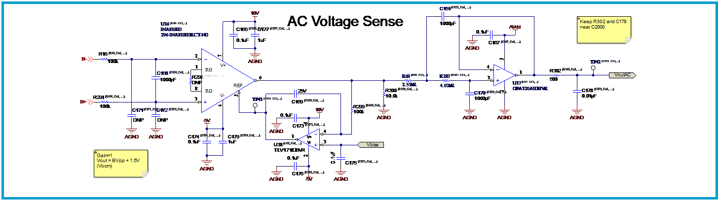
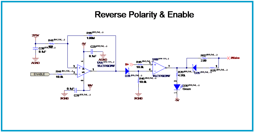
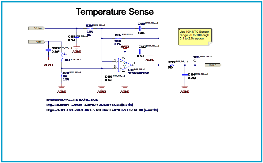
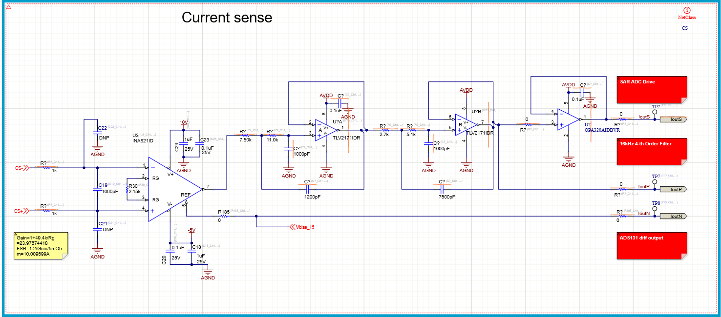
Other Parts Discussed in Thread: TIDM-DC-DC-BUCK, OPA320, OPA350, INA828, TMS320F280049, TMDSCNCD280049C, C2000WARE, ADS131M08, ADS1118, INA821, LM5106, ADS1119, TLV3702, TLV2171, TLV171, POWERSUITE

Hi,

I'm interested in TIDA-010086.... will this be available for order soon?

  • Lucas, hello.  Per our reference design deployment strategy, our reference designs are no typically available for purchase on ti.com. What we do is provide you, the customer, with the applicable design files such that you can build the design yourself and customize as is needed for your specific system.  I'm going to forward this request to the design owner to see whether he may have some sample inventory left over.  

    Best Regards,

    John Fullilove

    Reference Design Operations

  • Hi Lucas,

    We built limited number of hardware for this reference design. Presently we don't have stock to ship it to you. You can take a look at TIDM-DC-DC-BUCK reference design (orderable). The TIDM-DC-DC-BUCK reference design can achieve constant-voltage mode. For constant-current mode it will require some hardware change. 

    Regards,

    Shaury Anand

  • Hi,

    Not a problem.. I have gone ahead and customized the design with;

    • 8x NTC Remote temperature sensors
    • reverse polarity protection/slot output disable (deal diode one-way only)
    • RGBW LEDs for local operator feedback
    • Canbus to string a number of these together
    • I2C break out and an ESP32 for quick WiFi access.. (Yes I know, not a CC3220! ekk.)

    Current work in progress..;

    XTIDA-010086.pdf

    The outputs from the Current Sense and Voltage Sense aren't setup to directly drive a C2000 14-bit SAR ADC are they? It looks as if the voltage sense will be +-1.2v (in case of reverse connection) and that it'd need an OPA320 or OPA350 to drive each ADC input of the C2000, if I jumper those through to C2000 for cost reduction.

    Is my additions of AC voltage sense correct here? Trying to remove the DC offset so when I drive a 1kHz AC current into a cell I can capture the AC voltage directly, without software filters.. or even if I superimposed an AC signal ontop of the charging battery..  There may be a more economical way to drive this than using an INA828/818 but hey....

    Is this Reverse Polarity & enable connection sufficient? Tina shows good disconnect of cell connection when the positive connection goes negative, or when the CH_EN switch is tied to ground. I'm guessing the polarized caps on the outputs wont like being connected to a -4.2V @ > 100A supply...

    I've gone with using 8 SAR ADC channels to sample a buffered and "near linear" NTC sensor output. 20-100 degC capable... I'm not sure of the thermal conductivity of a TMP161 (or whatever digital sensor) on a flex pcb pushed against the side of a battery cell.. I'd rather a cheap inexpensive NTC that is already "springy".

    I've still a little to go before consolidating all these changes and bumping everything around before getting it made.

    ESD protection required on the battery terminal connections? as hands will be touching those areas, and what about the main 12V battery terminal connection, no reverse polarity or fuse on that connection. That could quickly toast the entire board. ekk.

    Lastly, would raising the switching frequency, lowering the inductor size and reducing the capacitor sizes drop the production costs? 250 or 300k switching frequencies possible with this cost pressure in mind?

  • Hi Lucas,

    Are are you planning to use F280049 control card? TMS320F280049 device only includes 12-bit SAR ADC. TMS320F28037x series includes both 12-bit and 16-bit ADC options. 16-bit mode will need a fully differential amplifier.

    C2000 internal ADC connection: Yes, you would need a precision op-amp to scale Isense /Vsense (-1.2V to 1.2V) to C2000 ADC input range. The board is not setup to use both external and C2000 internal ADC.

    You can find the control card pinmap in the SDK at below location. There are 21 ADC channels in F280049 100 pin device. C2000Ware_DigitalPower_SDK_3_00_01_00\c2000ware\boards\controlCARDs\TMDSCNCD280049C\A

    You can connect vsense_local to C2000 ADC and Vsense_remote to external ADC. You can use C2000 comparators for overcurrent protection.

    AC voltage sense circuit: I see you have connected a low pass filter at the output of OPA320A. A high impedance input will increase acquisition time. For 50 ohm or less source impedance, acquisition time is 75ns.

    You can design a 2nd order filter using below link.

    https://webench.ti.com/filter-design-tool/filter-type

    Besides in the ADS131M08 ADC, you can use DC block filter feature to sense only AC Vsense.

    Reverse polarity circuit: Your circuit seems right. Polarized cap cannot handle reverse polarity voltage. That's why protection circuit should be fast enough to disconnect the battery during fault. If you are planning overcurrent protection circuit in hardware, you can connect comparator output to this circuit.

    Temperature sense circuit: R219 will increase C2000 ADC acquisition time. It might be good idea to use CD4051 multiplexer for temperature sense. This will free up analog pins that you could use for overcurrent protection.

    You can also design a separate temperature sense module using ADS1118/9, so that you can use the same module for different types of battery test equipment.

    ESD protection: Adding a ESD diode will increase reliability of the circuit. You can also increase INA821 input resistance to 1k.

    https://www.ti.com/product/TPD1E10B06

    12V bus protection: I think this might not be needed for final design because it is a fixed connection and not accessible to user.

    Increase switching frequency: Increasing switching will reduce inductor and capacitor size. Smaller inductor will be cheaper and will also increase channel density. However it will come in expense of more power dissipation due to switching loss. Based on number of channels in the system you can calculate total power dissipation and design an appropriate cooling system.

    Other comments:

    The circuit has CC loop bandwidth of 180Hz when ISR is 16kHz. You need to optimize ADC input RC filter and increase ISR frequency to achieve 1kHz CC loop bandwidth. The reference design is tested in CCM mode. You can use LM5106, single input half bridge gate driver to reduce C2000 GPIO pins. The advantage of CCM mode is smaller ripple at low currents as compared to DCM mode. When using CCM mode, you will also need a local voltage sense feedback. The circuit will start with CV mode with local feedback and then enable switch is turned on to eliminate reverse current overshoot at the startup or during connect and disconnect of the battery.

    Tuning ADC clock frequency (fmod= 2^N time of switching frequency) will help in filtering of output ripple. The switching noise will coincide with notch frequencies of the sinc filter.

    Reduce ADC2 distance from control card connector, if you are providing clock from c2000. Keep as close as possible to avoid attenuation in the clock signal due long PCB trace.

    You can use EPWM or XCLKOUT pin of C2000 to synchronize multiple ADCs. See ADS131M08 datasheet 9.1.5 section for more details.

    Regards,

    Shaury Anand

  • AC Sense;

    Didn't realise the ADS131M08 had that feature.. easy. 

    Voltage and Current Sense;

    Seeing as the ADS131 input range is -1.3 to 2.5v (ish) I may aswell change the input inst amp for both the voltage and current to use a 1.5v reference with +- 1.2v for full range. Leaving a working input range for the C2000 of 0.3v to 2.7v which is within its 3v range. If I then input that reference voltage into one of the spare Analog pins I can do a differential in code? only 12-bit, but good for protection or comparators?

    Make the C2000 ADC pathway with a higher frequency pass through and keep the ADS131 for high precision V/I measurements, while using the C2000 to do the higher freq AC impedance sampling.

    Temp sensing;

    Dual ADS1119 on either side for the NTC sensing. Frees up all those analogs on the C2000 to run a full speed and be comparators/trips/protection/ac stuff.

    Software;

    is the SDK released yet with the TIDAs source code? not sure its in the current release version is all.

    Attached quick dirty analog input path? It allows the dual fuel of ADS131 and C2000 ADC usage. filters not calculated yet.

  • Voltage and Current Sense: I liked the idea to add common mode voltage of 1.5V. It will reduce an additional amplifier for c2000.

    Software filter to measure AC: The 12-bit C2000 ADC can achieve 11 bit ENOB at 100kHz input signal (see the TMS320F280049 datasheet for more information). That means you will get only 10 bit ENOB(0.1%) in either charge or discharge direction. This might not sufficient for this application.

    0.05% constant-current accuracy result in using C2000 12-bit ADC (shown in TIDA-010086 user guide), is when input of INA821 is multiplexed and C2000 uses all 12-bits for both charge and discharge direction.

    Software: It is not released yet . I can share the code with you over email

  • CC/CV control loop; ADS131M08 current sense

    U/OVP; C2000 ADC

    OCP; C2000 ADC

    Reverse battery insertion; tlv3702 dual V comparator with single fet. I use a 4-wire slot used that guarantees Vsense connection before PGND and +VBat.

    Impedance measurement is done only between 20% 16bit V and I should already be sampled . An 8x or higher sample rate to impedance frequency is sufficient to sample the quadrants of Icos Vcos Isin Vsin. The beauty is being able to sample multiple wavelengths for increased data .

    ... Just realized the schematic literally says 28379, meaning this was developed on a F28379D or S C2000 chip.. no matter.

    All 8 comparators mapped in and using two PWM modules to generate the seperate ADC clocks. I've added clock buffer to each one too. Hmm

  • Couldn't the ADS131 and C2000 be driven from the same filter path given a 1.5v common ? would it be best to add an OPA320 to drive the C2000 SAR ADC and connect the ADS131 to the output of the second part (B) TLV2171.

    INA821 -> TLV2171 (A) -> TLV2171 (B) -> ADS131 (+ = out; - = 1.5vRef) 

    INA821 -> TLV2171 (A) -> TLV2171 (B) -> OPA320 -> C2000 Analog pin

    the DNP marked filter circuit has a -3db of 16kHz

    The AFR for current sense would then look like;

  • Updated schematic with separate Vsense for B+ and Vesne+ using either a  TLV171 or INA821 for the 4-wire battery hookup. the 4-wire hookup needs special attention because of the common mode noise being injected into the battery directly pushing the Vsense nodes.

    Moved the Vsen / Isen for the C2000 to their own driven single ended connections. VsenS = 2.4v @ 5.0v bat.. so scaled up nicely. VsenP/N is still 1.2v at a 1.25v bias. 

    Added the 4th order filters to all pathways. Tina agrees with me...

    Now the C2000 has the VsenS and IsenS analog signals driven onto pins with comparators and to pins that exist on the F280049C controlCard socket.

    I have yet to check the clock of the ads131m08 to ensure its driven sufficiently fast enough to get a 1khz bandwidth CC control loop..

    Did I miss anything?

    TIDA-010086_mod2.pdf

  • Hi Shaury,

    Will you release the ref source code for TIDA-010086, I can't find the project in DigitalPower software development kit ?

    Tony

  • email: lucas.oldfield@gmail.com please :) ta

  • Hi Shaury,

    Pls send the ref code to me ,thanks!

    tornado2000cn@msn.com

    Tony

  • Hi Lucas,

    Control card connector is same for all C2000s. TMS320F28379D control card uses both J5 and J6, while F280049 only uses J5. I had developed code on F280049, which has less number of GPIOs as compared to F28379D.

    While routing ADC clock signals and SPI trace,  reduce the trace length to avoid attenuation in amplitude. I had observed some attenuation in ADC CLK 2 amplitude on the board due to unused stub on the PCB.

    Regards,

    Shaury

  • I've remapped the Control Card connector pin-out for the F28379D as it has double the MHz and twice the cores. Plenty of clock speed to develop on.

    As the the clocks, I can use two separate PWM modules clocking into separate SN74LVC2G1 buffers. This should be sufficient to guard against signal attenuation. 

    There are 8 available comparator positive connections for the IoutS[1..8] connections for OCP UCP hardware tripping of the PWM functions, and the V and I measurements if using the C2000 are spread across four ADC 12 bit modules. That's plenty of measurement bandwidth, and throw in a mid-point reference across all ADC via A0. its 5 channels per ADC.

    I think I have enough to go from now, a code-share will help but it does look like there is enough doco and examples on the other projects in the powerSuite to work from ;) cheers.

  • Hi Lucas,

    Regarding your question about filter and bandwidth:

    The feedback path should attenuate inductor current ripple noise below 0.01%. Otherwise you will see error in the average current when the battery voltage changes. For switching frequency of 100kHz, 12V vin, 5V 47uH inductor, you will get about 600mA inductor current. To reduce current ripple noise below 1mA, we need >55 dB attenuation.

    ADS131M08 has a digital 3rd order sinc filter. You can see below ADS131M08 provides greater >60B attenuation at 100kHz when output data rate is 32ksps. So you can achieve less than 0.01% current control accuracy without any additional filtering in ADS131M08 feedback path.

    However you would not get same level attenuation when using C2000 12-bit ADC after averaging. We need a filter in the C2000 feedback path if we want to use it for current control.

    ADS131M08 datasheet figures:

    Synchronous buck current AC model: You can approximate the power stage as L and R series circuit, where L is buck converter inductor and R is total impedance to ground. I have attached analog CC loop simulation below. You can implement discrete constant current CC loop in MATLAB to verify the system bandwidth. 

    /cfs-file/__key/communityserver-discussions-components-files/234/Sync_5F00_buck_5F00_CC_5F00_control.TSC

    You can check the following path in the SDK for controlCard pin map details:

    C2000Ware_DigitalPower_SDK_3_00_01_00\c2000ware\boards\controlCARDs\TMDSCNCD28377D\R1_1_A

    Let me know if you have any questions. If I have answered all of your questions, please click on "Resolved" button.

    Regards,

    Shaury

  • Yes, you can also check digital power buck converter example in the SDK

    C2000Ware_DigitalPower_SDK\solutions\tidm_dc_dc_buck

  • Perfect. I was only intending to use the C2000 Comparators for current protection, the ADS131 for CC and CV control. thanks for you answers. Sweet...

  • Okay Lucas! I see that sinc3 filter response got deleted in my previous reply. I'm attaching it again in this reply.

    ADS131M08 datasheet: Figures 25 and 26