This thread has been locked.

If you have a related question, please click the "Ask a related question" button in the top right corner. The newly created question will be automatically linked to this question.

WEBENCH® Tools: ADS8860IDGS

Other Parts Discussed in Thread: ADS8860, LM6144, OPA320, LM1117

Tool/software: WEBENCH® Design Tools

Dear Sir/Madam,

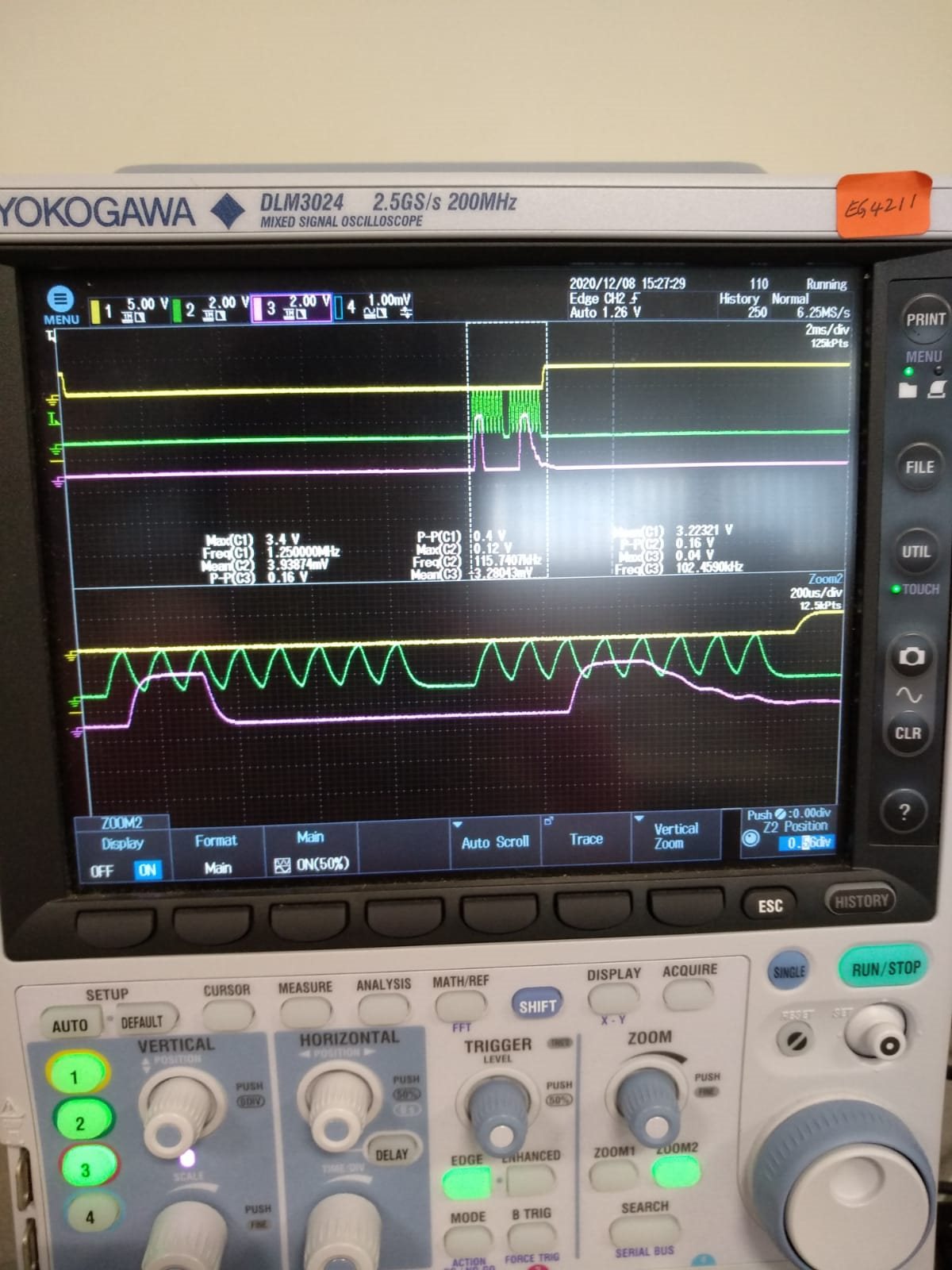
I use 16bit ADS8860 to interface with esp32 Wroom. Today, when I test the ads8860 with 1.5V dc and I check Convst, SCLK and Dout signal in oscilloscope, I find out that the CLK frequency that I set in ESP32 code doesn't match with Oscilloscope readings. I set 10kHz clk frequency in ESP32 code, but clk frequency of 115.740kHz is shown in oscilloscope. 

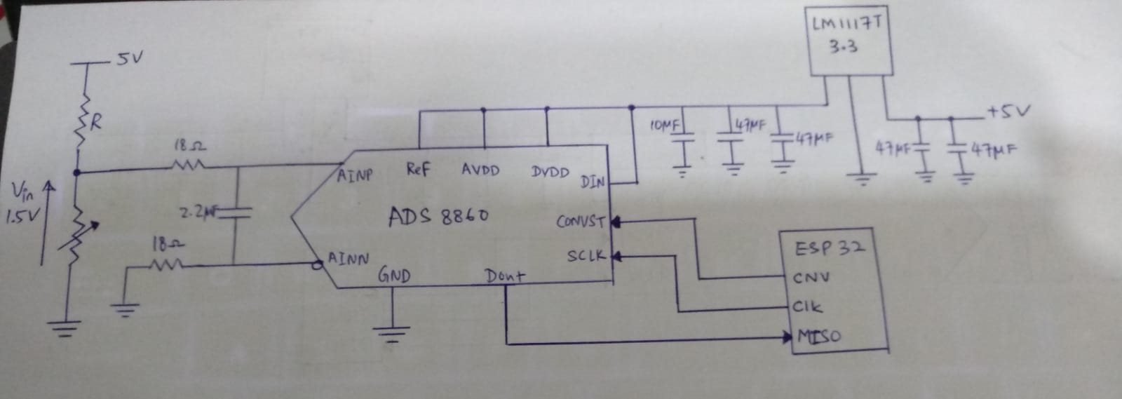
Detail circuit connection between ESP32 and ADS 8860 is shown below.

Below image shows the Convst (yellow), CLK signal (green), and Dout (pink) read in oscilloscope. From the figure, the clk frequency is read as 115.740 kHz instead of 10kHz. I am not sure whether the problem is due to ESP32 microcontroller or my circuit connection has issue. 

Q1. Can you suggest what could be the possible reason?

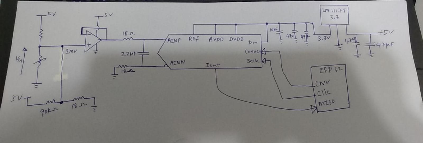
Next, when I change the input voltage to 150 uV DC, the Dout signal is measured zero. The detail circuit diagram is shown below.

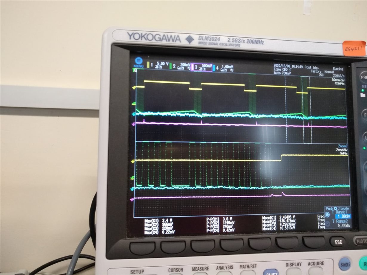
Q2. Below image shows the Convst (yellow), CLK signal (green), and Dout (pink) read in oscilloscope. From the figure, the Dout signal is zero and ESP 32 microcontroller is read as 0V. Based on the calculation, ADS8860 should be able to convert the analog input voltage as low as 50 uV (3.3V/65536). Therefore, I would like to check whether my current circuit connection is correct? If my current circuit connection is wrong, where did I make mistakes? and how to correct those mistakes? so that I can use full input voltage range.

Last, but not least, in above oscilloscope figure, the CLK frequency is 1kHz. But, the clk signal (green color) looks like saw tooth waveform. Therefore, I would like to know why the clock signal looks like saw tooth wave?

Thanks.

  • Hello, Q1. You appear to be getting measurement errors with your scope. If you look at the zoom portion of the CLK, the time scale is 200uS and you have two clock periods. This is equal to 10kHz. Q2. The ADS8860 has an offset specification of +/-1mV typical. This means that you cannot measure voltages less than this value with every part. You will need to add an amplifier that can add an offset voltage so that the ADC can measure inputs less than 1mV Q3. This appears that your MCU is setting the clock pin to hi-z, or letting it float between readings. This could also be a measurement error if you have the scope channel set to AC coupling. I suggest you apply a larger voltage to the input, such as 1V. Then see if the ADC output result is close to this voltage to confirm that you have communications to the device working correctly. Regards, Keith Nicholas Precision ADC Applications
  • Dear Mr. Nicholas,

    Thank you for your reply.

    I would like to clarify your answer to Q2. You said that I need to add an amplifier which can add offset voltage of 1mV to Vin to be able to measure Vin less than 1mV. 

    I add summing amplifier at the input (see below schematic diagram). Could you help me check my schematic diagram whether it is right?

    Lastly, in my code, do I need to subtract the offset value of 1mV in order to get back actual input voltage? For example, assume Vin = 150uV. After I add 1mV offset to Vin, voltage at AINP of ADS8860 will be 1.15mV. So, in the ESP microcontroller program, do I need to do following ?

    V_measure =  (ADC reading * 3.3V / 65536) - 1mV 

    Thanks, 

    Susan

  • Hello Susan,

    The approach you have taken will add an offset voltage that changes with the input resistance.

    What is the range of Vin that you would like to measure?  What is the input resistor network value? 

    If you would like to measure inputs from 0V (with 54uV resolution) up to 3.3V, then the following amplifier configuration should work.  This circuit will add an offset as well as a small gain change to keep the voltage inside the range of the ADS8860.

    In software, you will need to adjust both the offset and the gain.

    V_measure =  1.064516*[(ADC reading * 3.3V / 65536) - 100mV ]

    Regards,
    Keith

  • Dear Mr. Nicholas,

    Thank you for your reply.

    I would like to have my input voltage range to be 60uV to 3.3V.

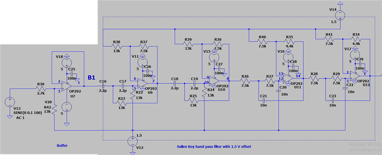
    Below schematic diagram shows the whole the circuit connection from MEMs vibration sensor > Buffer > Band pass filter > Summing Amp > Charge-kickback Filter > ADS8860.

    I am using LM6144 Rail-to-Rail input- output op-amp instead of OP292. The lower cut-off frequency of band pass filter is 10Hz and the higher cut-off frequency of band pass filter is 1.5kHz.

    Could you please suggest the summing amplifier configuration for ADS8860 for the input voltage range from 60uV to 3.3V? Can I use the summing amplifier configuration that you suggested in previous post? because that summing amplifier configuration can accept Vin range from 0V to 3.3V and I only need minimum input voltage of 60uV.

    Lastly, could you help me check whether my current circuit configuration can support sampling frequency 10kHz? I am using 3 wire configuration with SPI CLK frequency of 200 kHz.

    Thanks,

    Susan.

  • Dear Mr. Nicholas,

    Today, when I test the ADS8860 with AC input from function generator, I find out that the ADC conversion result is wrong.

    The Block diagram of circuit connection is shown below. The detail schematic diagram of each block is shown in my previous posts.

    •The SPI clk frequency is 400kHz, and sampling frequency is 5kHz. The ADC reading is converted into voltage by using - ADC reading *(3.3/65536). Then, I collect the ADC reading for 1sec. After that, I do Fast Fourier Transform in MATLAB to check for magnitude spectrum.
    •The time signal and magnitude spectrum are shown below. The right hand side image is the signal at the output of low pass filter. The middle image is the ADC readings collected by ESP32. The left hand side image is the magnitude spectrum of ADC reading in MATLAB. In the magnitude spectrum, the frequency and amplitude results are wrong.
    •In the previous posts, you suggested to add “summing amplifier” to add 1mV offset error of ADS8860. However, I don’t know how to do it.  My input voltage can vary from 60uV to 3.3V.
    Therefore, could you suggest how to build summing amplifier for my current issue?
    Thanks,
    Susan
  • Hi Susan,

    Since you have a bandpass filter, you can simply adjust the gain of the filter to keep the input range of the ADC within an acceptable range.

    Your above waveform on the right looks like a 10mVpp signal, but your acquired waveform is saturated, which implies the input to the ADC is more than 3.3Vpp.

    Please make sure your input amplifiers are providing the correct amplitude levels.  The output of the filter amplifier should have a waveform in the range of 1.5V+/-1.4V, or 0.1V to 2.9V.  This will use most of the available full scale input range of the ADC and provide good results.

    1.  Please look at the front end amplifier and adjust the gain so that the full scale output of the filter amplifier is in the range of 0.1V to 2.9V.  (+/-1.4V with a 1.5V DC bias)

    2.  After you are able to get a correct input amplitude, we can then look at the ADC.   SCLK=200kHz will support a sample rate of 10ksps.

    3.  Please change the input capacitor on the ADC from 2.2uF to 2.2nF.  2.2uF is too large and will not settle at 10ksps.

    Regards,
    Keith

  • Hi Nicholas,

    Previously, I clicked the "This resolved my issue" button wrongly. The issue hasn't resolved yet.

    I have edited my circuit and tested the circuit in TINA software and in practice. The output of the circuit is within 0.2V to 3.0V for input AC voltage range of +/-260mV. Bandwidth of the filter is 10Hz to 1kHz.

    Schematic diagram of whole circuit

    Simulation result - Vin = +/-260mV.

    I have a few questions for hardware setup.

    Q1. In figure 63 of datasheet, there is the buffer circuit before charge kick-back filter. So, I would like to know whether I need to place buffer at the output of my circuit ?

    Q2. Can I use the same resistor and capacitor values given in figure63 of datasheet in my application [I would like to measure vibration data from MEMs sensor at 5kS/s] ? 

    Q3. I can't find 5 m ohm resistors. Are there any alternatives resistance values for REF6003 driver?

    Q4. Instead of using REF6003 reference driver, if I connect LM1117T (3.3V output) to AVDD, DVDD, DIN and REF pin of ADS8860, what should max SPI clk rate and data sample rate be?

    Next, for software setup - 

    Q5. what does SPI data mode that ADS8860 support? because there are 4 different SPI data modes and I couldn't find what SPI data mode is supported by ADS8860 in datasheet.

    Q6. What is the bid order of ADS8860 (MSB first or LSB first)?

    Q7. According to 3-wire communication timing diagram, can I read the whole 16 bits at 1 time by using "SPI.transfer16(val16)" in Arduino IDE?

    Q8. According to Arduino SPI library, SPI transfer function "SPI.transfer(val)" requires the byte to send out over the bus and the function will return the received data. Therefore, what should be the input parameter to the "SPI.transfer" function?

    Q9. Are there SPI communication examples of ADS8860 using Arduino SPI library  because I couldn't get SPI communication between ADS8860 and ESP32 wroom get working? Therefore, I would like to check my Arduino IDE code with reference.

    Sincerely,

    Susan 

  • Hello Susan,

    1.  The ADS8860 example design using OPA320 and the charge kickback filter components has been built and tested to meet full performance of the ADC.  You could eliminate this if operating at a lower sample rate, but it would require design and simulation effort to determine the maximum sample rate, and the correct values of the charge kickback filter.  I suggest you keep the OPA320 and the values to get predicted performance from the ADC.

    2.  You can only use these values if using the OPA320.  If not, you will need to adjust these values, and likely lower the ADC sample rate, for good performance.  Please refer to TI Precision Labs - ADC's, section 6 for details on how to design this section.


    https://training.ti.com/ti-precision-labs-adcs-introduction-sar-adc-front-end-component-selection?context=1139747-1140267-1128375-1139106-1128643

    3.  The 5mOHM on the SS pin is an error, you can use 120kohm for this resistor.  For the 5mohm in series with the 47uF output capacitor, you can use any value between 20mOhm and 100mOhm.  5mOhm is not recommend when using 47uF.

    4.  The SPI CLK frequency is independent of sample rate.  If you directly drive the reference pin with the LM1117, you will probably need to reduce the sample rate to less than 10ksps, but you would need to run a detailed analysis in SPICE, or build and test, to determine the exact requirements.

    5.  SPI MODE 00

    6.  The first launch bit in a frame is D15, so MSB first.

    Questions 7,8,9   We do not have any code examples for Arduino, and I am not familiar with the syntax in order to answer your questions.  I suggest posting any Arduino specific questions on the Arduino question and answer forums.

    However, the ADS8860 does not have any internal registers.  Since the Arduino will output data on the MOSI pin, you can just write 0x0000h in this case.  In order to transfer the data, you need a single 16b (16 SCLK) transfer frame, or a total of 2 bytes.

    Regards,
    Keith