This thread has been locked.

If you have a related question, please click the "Ask a related question" button in the top right corner. The newly created question will be automatically linked to this question.

PMP8740: Full Bridge Output Noise and Ripple

Part Number: PMP8740

Hi Roberto ,

I have designed AC-DC battery charger by taking PMP8740 as a reference. I used same schematics like PMP8740 both full bridge and PFC circuits but in PCB layout I have made some changes like PCB size.

My pfc and full bridge circuits working but I have some problems with these circuits.

Now I am testing only my full bridge circuit.

The full bridge input is 400 volt 5A external dc power supply. Not the PFC output

When no load Full Bridge output is 27,3V approx.

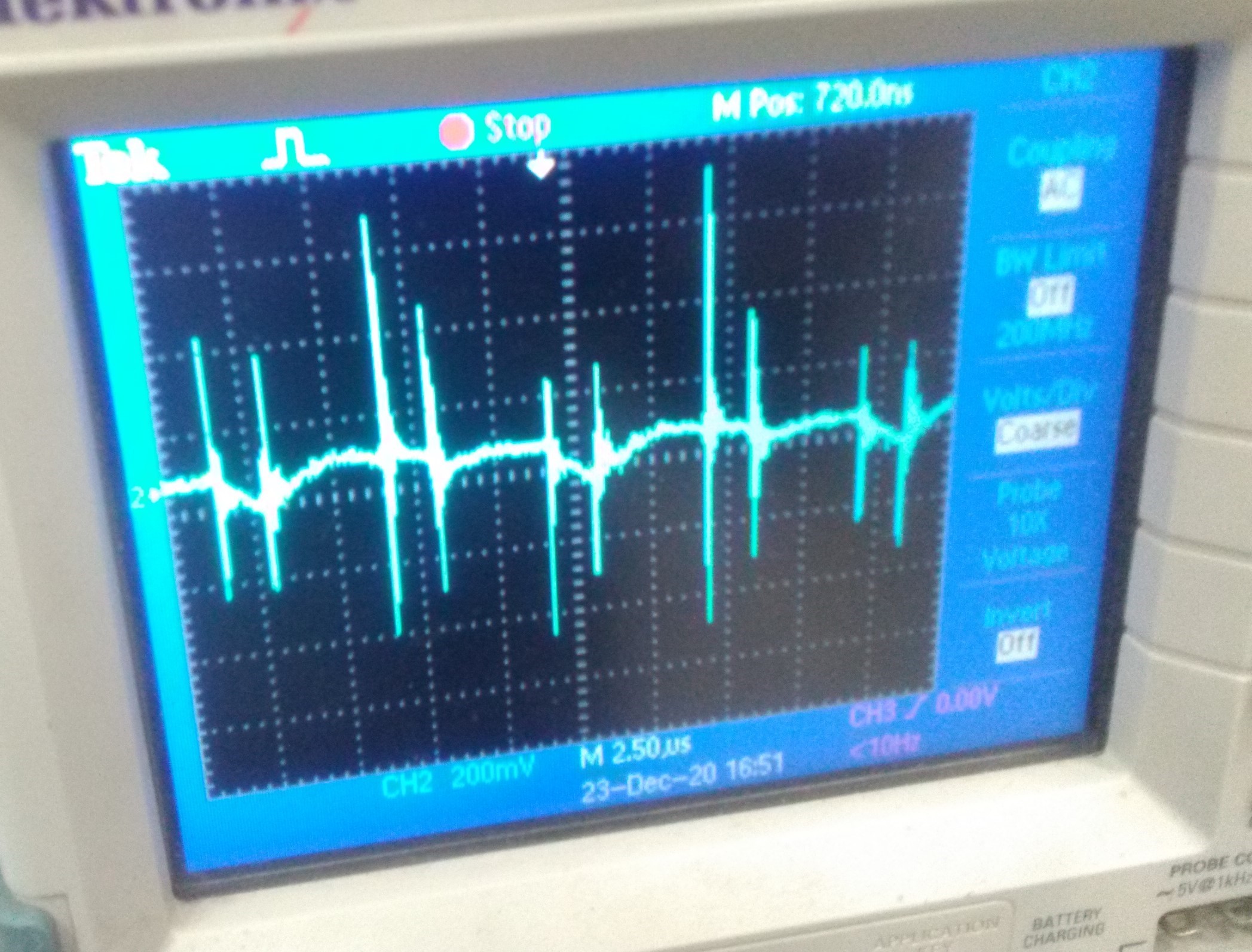
When 50A load , output is 27,1 volt and output has high frequency noise (1.2 Volt peak to peak) and ripple. I attached the scope view in figure 1.

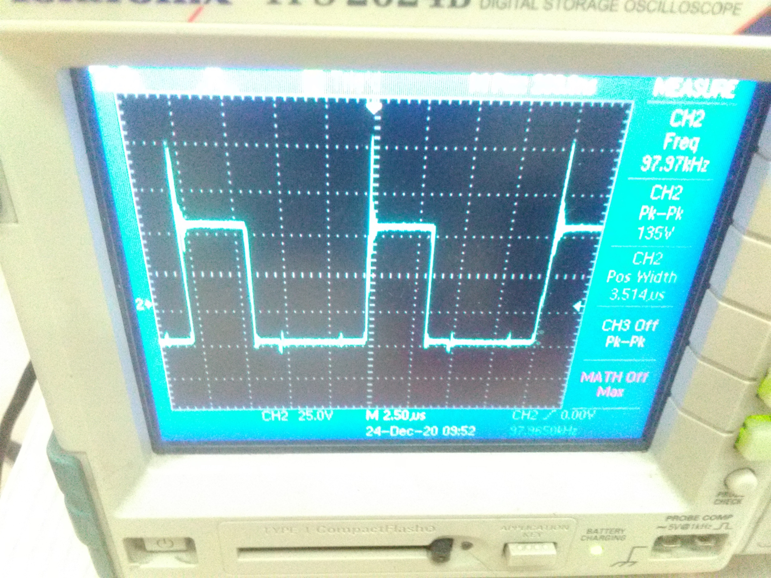
Also I have observed the Q23 Vds( PMP8740 schematic) drain source voltage in figure 2.  In my opinion these hf noise comes from full bridge transformer secondary winding.

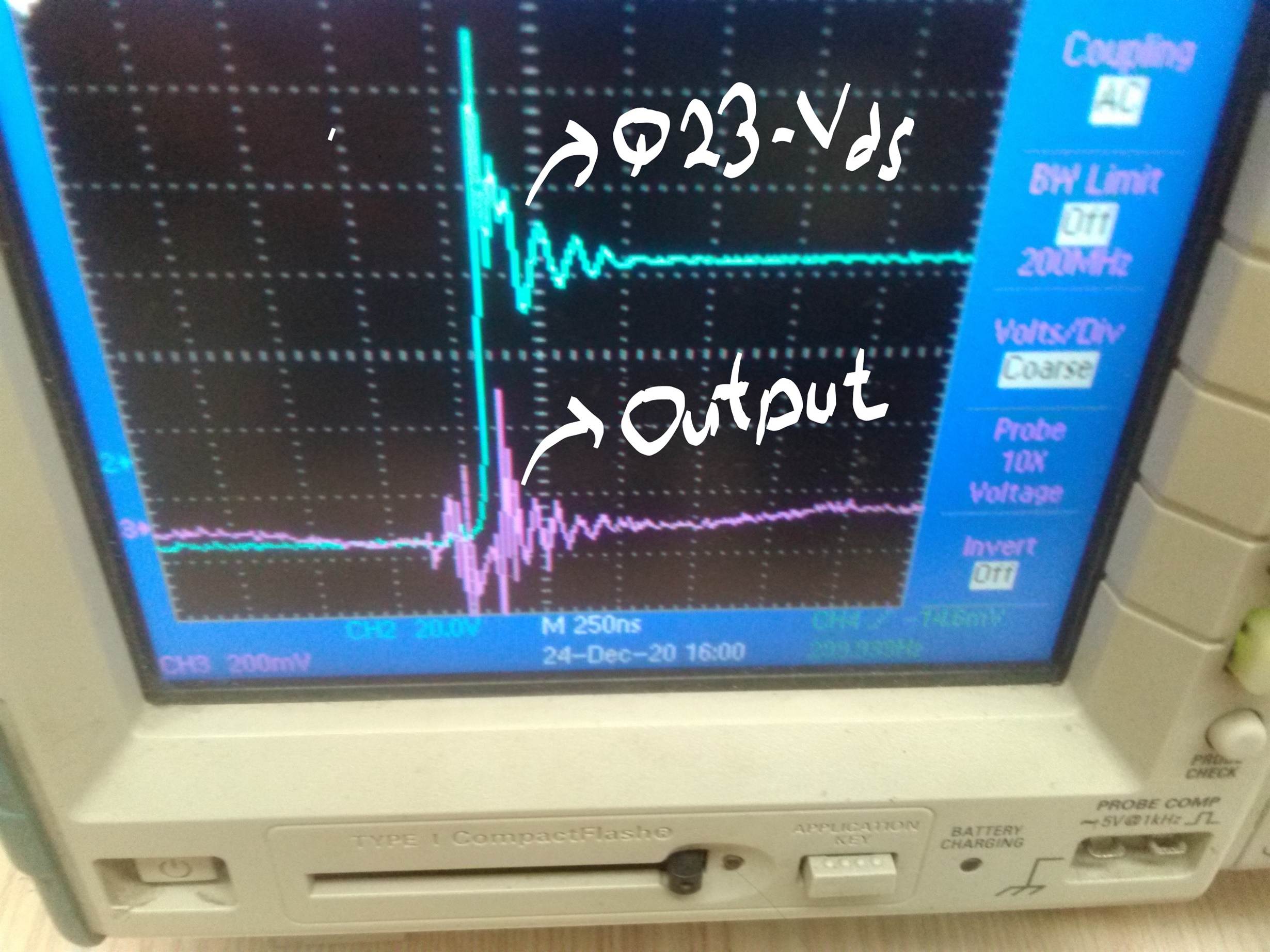
I have observed the Full bridge output and Q23 Vds in scope together in figure 3.

How can I reduce output noise?

what could be sources of noise?

Figure1 :

Figure 2:

Figure 3:

  • Hello,

    The person who made this reference design is out on holiday. Thanks for your understanding. 

  • Hi Pradeep,

    Thanks again for redirecting.

    Hello Bilgin,

    I agree with you that the noise you are measuring on the output depends on the ringing you observed on the Q23 switch-node.

    In order to reduce this noise, I suggest to damp both switch-nodes (Q23 and Q22) by fine tuning the snubber RC networks R125...R128 and C100...C103. These values depend on the leakage inductance of the transformer as well as the board layout.

    Other parameters, responsible of this ripple and noise, are:

    1) ESR and ESL values of all electrolytic capacitors. If you used the part numbers I employed, you should not have any problem.

    2) Position of C58 and C59 (ceramic capacitors): these should be placed very close to the output connector

    3) Interwinding capacitance (turn to turn) in the inductor L2; this is more difficult to control, and you may need to use another inductor, which changes the layout and cost & space on the board. I would use this in case there is no improvement in any other way.

    By taking into account all these concepts, you should be able to measure values close to what I saw on my prototype, which was ~ 250 mV(pk-pk).

    Best regards,

    Roberto