This thread has been locked.

If you have a related question, please click the "Ask a related question" button in the top right corner. The newly created question will be automatically linked to this question.

TIDA-010056: Interfacing Problem between MCU and GATE driver circuit

Part Number: TIDA-010056
Other Parts Discussed in Thread: MSP430FR2355, MSP430FR4133, , DRV8350R, DRV8353

Hello TI Helpers,

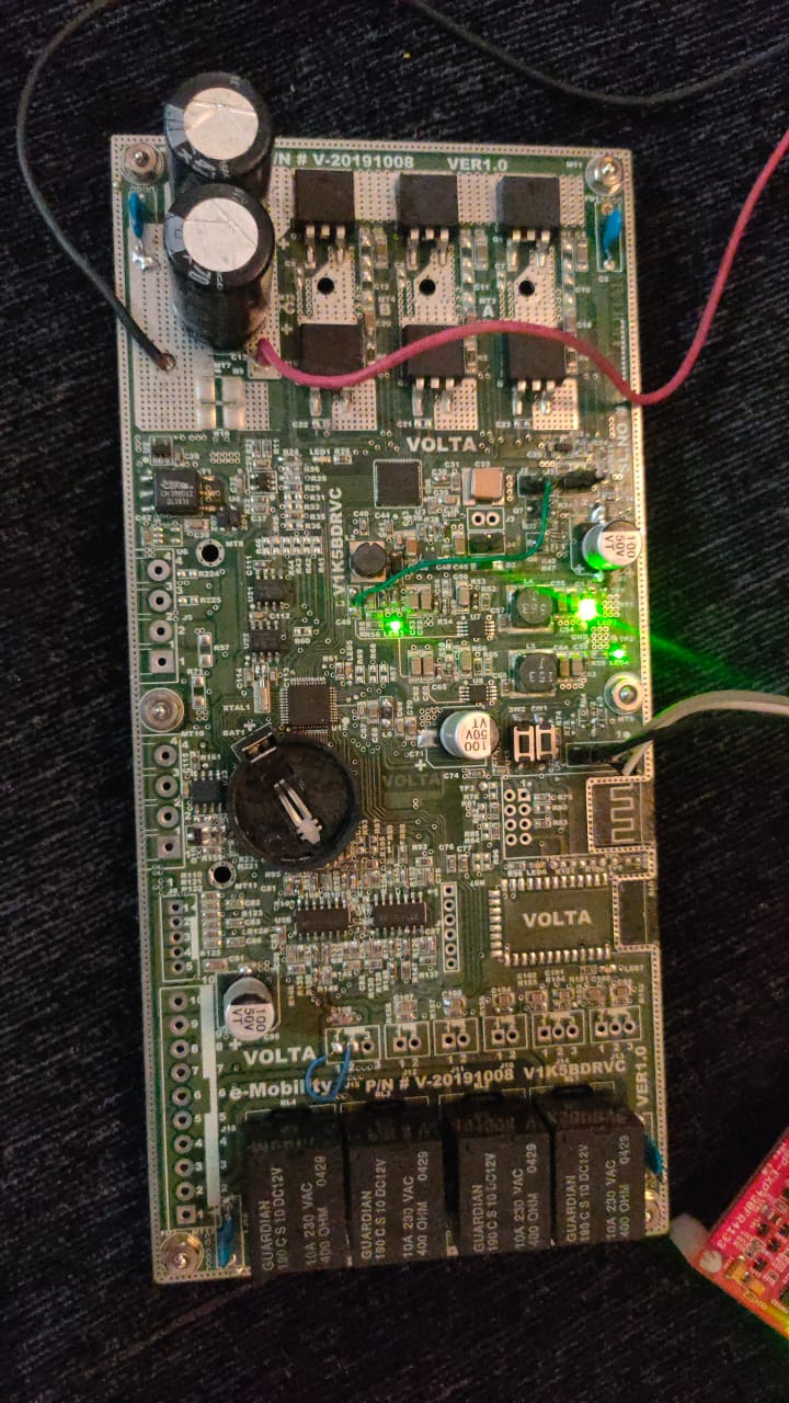
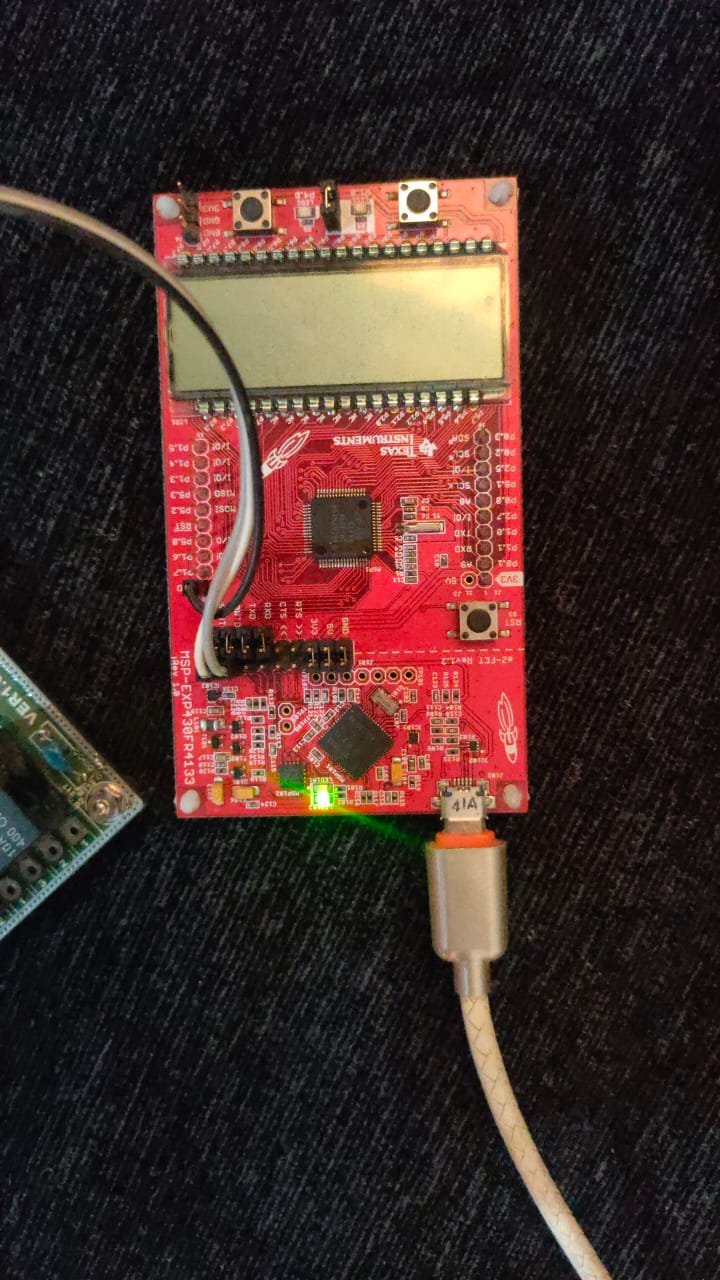
I'm using CCS version 10.1.1.00004 . I have MSP430FR4133 launchpad used as burner  into my controller which has MSP430FR2355 MCU and gate driver circuit (DRV8353RH). I am working on BLDC motor controller. I have TIDA-010056_Firmware_1.0 code which i am using for my project and i give 24v using adapter to controller. I am able to burn code into my controller but i didn't get any voltage across MOSFETs(inverter circuit).i do not connect BLDC motor yet. I want 20v across MOSFETs but didn't get it. Is there any interfacing problem??? please help me?!

Thank you in advance.

  • Hello Sudhir,

    Can you share your schematic file for us to look at?

    Which motor driver are you using? Is it the same one as in TIDA-010056 (DRV8350R)?

    Please check if the driver is powering ON by measuring the voltage at DVDD, VCP, and VGLS.

    Thanks,

    Matt

  • We are using DRV8353RH as driver circuit in our hardware where as  we're using TIDA-010056 (DRV8350R) in software part...is it create problem??

  • Hello TI Helpers,

    Can you tell us, how to check voltage at DVDD, VCP and VGLS ?

    Thank you in advance.

  • /* --COPYRIGHT--,
     * Copyright (c) 2019, Texas Instruments Incorporated
     * All rights reserved.
     *Modified by : A0132403
     *Modified Date: 30th April 2019
     *Modified  * Redistribution and use in source and binary forms, with or without
     * modification, are permitted provided that the following conditions
     * are met:
     *
     * *  Redistributions of source code must retain the above copyright
     *    notice, this list of conditions and the following disclaimer.
     *
     * *  Redistributions in binary form must reproduce the above copyright
     *    notice, this list of conditions and the following disclaimer in the
     *    documentation and/or other materials provided with the distribution.
     *
     * *  Neither the name of Texas Instruments Incorporated nor the names of
     *    its contributors may be used to endorse or promote products derived
     *    from this software without specific prior written permission.
    
     * THIS SOFTWARE IS PROVIDED BY THE COPYRIGHT HOLDERS AND CONTRIBUTORS "AS IS"
     * AND ANY EXPRESS OR IMPLIED WARRANTIES, INCLUDING, BUT NOT LIMITED TO,
     * THE IMPLIED WARRANTIES OF MERCHANTABILITY AND FITNESS FOR A PARTICULAR
     * PURPOSE ARE DISCLAIMED. IN NO EVENT SHALL THE COPYRIGHT OWNER OR
     * CONTRIBUTORS BE LIABLE FOR ANY DIRECT, INDIRECT, INCIDENTAL, SPECIAL,
     * EXEMPLARY, OR CONSEQUENTIAL DAMAGES (INCLUDING, BUT NOT LIMITED TO,
     * PROCUREMENT OF SUBSTITUTE GOODS OR SERVICES; LOSS OF USE, DATA, OR PROFITS;
     * OR BUSINESS INTERRUPTION) HOWEVER CAUSED AND ON ANY THEORY OF LIABILITY,
     * WHETHER IN CONTRACT, STRICT LIABILITY, OR TORT (INCLUDING NEGLIGENCE OR
     * OTHERWISE) ARISING IN ANY WAY OUT OF THE USE OF THIS SOFTWARE,
     * EVEN IF ADVISED OF THE POSSIBILITY OF SUCH DAMAGE.
     *
    ***********************************************************************************
    // System Configuration
    // Device Part Number   : MSP430FR2355
    // compiler             : Code Composer Studio v8.3.0
    // Oscillator Frequency : 24MHz,  using internal DCO
    // PWM generation       : TIMER: TB3.1 �TB.6, Clock = 25 MHz, PWM frequency set for 20kHz
    20 kHz
    //
    // Position Feedback    : Hall sensors signals
    //                        HA -> P3.0
    //                        HB -> P3.1
    //                        HC -> P3.2
     *
    // ADC                  : A0 -> Speed reference from the external potentiometer/trigger
    //                        A6 -> Phase A back EMF sensing for sensorless
    //                        A5 -> Phase B back EMF sensing for sensorless
    //                        A4 -> Phase C back EMF sensing for sensorless
    //                        A7 -> DC bus voltage sensing
    //                        A8 -> Low-side DC bus current sensing
    //                        A9 -> PCB or FET temperature feedback
     *
     *
    //Comparator configuration for back EMF zero crossing detection             : CB2/P1.2 -> IDC
    //                      COMP0.O (P2.0) � Phase A back EMF zero cross comparator
    //                      COMP1.O(P2.1) � Phase C back EMF zero cross comparator
    //                      OA1O (P1.5) - Phase C back EMF zero cross comparator. The
    //opamp of smart compo module is configured as a comparator
    *
    //DRV8350RS - SPI programming pins connection
    //                      P4.4 -> SCS
    //                      P4.5 -> SCLK
    //                      P4.6 -> SDO
    //                      P4.7 -> SDI
     *
    //UART communication
    //                      P4.2 -> UART RX pin
    //                      P4.3 -> UART TX pin
    //MCU Digital Inputs/Output
    //                      P5.4 -> Direction of motor rotation
    //                      P4.1 -> ENABLE connection for DRV8350R
    //                      P4.0 -> FAULT pin connection from DRV8350R
    //                      P2.6 -> LED output
    
    ***********************************************************************************/
    
    //Header Files//
    #include "msp430fr2355.h"
    #include "stdint.h"
    
    #define CALTDH0CTL1_256        *((unsigned int *)0x1A36)
    
    /*****************************InstaSPIN**************************************/
    
    
    #define         PWM_PERIOD                  600  //PWM Frequency (Hz) = 25MHz/((2*PWM_PERIOD)-1)
    #define         MAX_DUTYCYCLE               600  //relative to PWM_PERIOD
    #define         MIN_DUTYCYCLE               5    //relative to PWM_PERIOD
    #define         ACCEL_RATE                  100  //Ramp up time to full scale duty cycle = (Full scale duty cycle) * ACCEL_RATE * PWM_PERIOD/PWM_Frequency
    #define         DEAD_TIME_MCU               1   // Dead time from MSP430 = DEAD_TIME* 0.0625 uS (for 16MHz clock)
    #define         Block_Rotor_Duration        800  //Blocked_rotor shut off time (s) = Block_Rotor_Duration*30000/Timer clock frequency
    
    /*************************************program variables**********************************************/
    unsigned int DC_BUS_CURRENT = 0;
    unsigned int DC_Bus_Voltage = 0;
    unsigned int SPEED_REF = 0;
    unsigned int Temperature_feedback = 0;
    unsigned int start_count = 0;
    unsigned int HALL_STATE = 0;
    unsigned int softstart_counter = 0;
    unsigned int CurrentDutyCycle = 100;
    unsigned int DIRECTION = 0 ;
    unsigned int FirstADC_flag = 1;
    unsigned int ADC_selection_flag = 1;
    unsigned int ADC_selection_flag_1 = 1;
    unsigned int Block_Rotor_Counter = 0;
    unsigned int Block_Rotor_Counter_1 =0;
    unsigned int ADC_RESULT = 0;
    
    unsigned int commutation_time = 0;
    unsigned int commutation_time_counter = 0;
    unsigned int advance_angle_time_counter = 0;
    unsigned int advance_angle_time = 0;
    unsigned int commutation_done = 0;
    unsigned int Previous_State = 0;
    unsigned int Present_State = 0;
    unsigned int PWM_DUTY = PWM_PERIOD;
    
    
    /*******************************ADC channel selection*******************************************/
    
    
    #define MEASURE_SPEED                                                                   \
                                    ADCCTL0 |= ADCSHT_2 | ADCON;                            \
                                    ADCCTL1 |= ADCSHP;                                      \
                                    ADCCTL2 &= ~ADCRES;                                     \
                                    ADCCTL2 |= ADCRES_2;                                    \
                                    ADCMCTL0 |= ADCINCH_0;                                  \
                                    ADCIE = ADCIE0;
    
    #define MEASURE_TEMP                                                                    \
                                    ADCCTL0 |= ADCSHT_2 | ADCON;                            \
                                    ADCCTL1 |= ADCSHP;                                      \
                                    ADCCTL2 &= ~ADCRES;                                     \
                                    ADCCTL2 |= ADCRES_2;                                    \
                                    ADCMCTL0 |= ADCINCH_9;                                  \
                                    ADCIE = ADCIE0;
    
    #define MEASURE_VDC                                                                     \
                                    ADCCTL0 |= ADCSHT_2 | ADCON;                            \
                                    ADCCTL1 |= ADCSHP;                                      \
                                    ADCCTL2 &= ~ADCRES;                                     \
                                    ADCCTL2 |= ADCRES_2;                                    \
                                    ADCMCTL0 |= ADCINCH_7;                                  \
                                    ADCIE = ADCIE0;
    
    #define MEASURE_IDC                                                                     \
                                    ADCCTL0 |= ADCSHT_2 | ADCON;                            \
                                    ADCCTL1 |= ADCSHP;                                      \
                                    ADCCTL2 &= ~ADCRES;                                     \
                                    ADCCTL2 |= ADCRES_2;                                    \
                                    ADCMCTL0 |= ADCINCH_8;                                  \
                                    ADCIE = ADCIE0;
    
    #define MEASURE_BEMF_A                                                                  \
                                    ADCCTL0 |= ADCSHT_2 | ADCON;                            \
                                    ADCCTL1 |= ADCSHP;                                      \
                                    ADCCTL2 &= ~ADCRES;                                     \
                                    ADCCTL2 |= ADCRES_2;                                    \
                                    ADCMCTL0 |= ADCINCH_6;                                  \
                                    ADCIE = ADCIE0;
    
    #define MEASURE_BEMF_B                                                                  \
                                    ADCCTL0 |= ADCSHT_2 | ADCON;                            \
                                    ADCCTL1 |= ADCSHP;                                      \
                                    ADCCTL2 &= ~ADCRES;                                     \
                                    ADCCTL2 |= ADCRES_2;                                    \
                                    ADCMCTL0 |= ADCINCH_5;                                  \
                                    ADCIE = ADCIE0;
    
    #define MEASURE_BEMF_C                                                                  \
                                    ADCCTL0 |= ADCSHT_2 | ADCON;                            \
                                    ADCCTL1 |= ADCSHP;                                      \
                                    ADCCTL2 &= ~ADCRES;                                     \
                                    ADCCTL2 |= ADCRES_2;                                    \
                                    ADCMCTL0 |= ADCINCH_4;                                  \
                                    ADCIE = ADCIE0;
    
    #define CONVERSION_ENABLE                                                               \
                                    ADCCTL0 |= ADCENC | ADCSC;
    
    #define CONVERSION_DISABLE                                                              \
                                    ADCCTL0 &= ~ADCENC;                                     \
                                    ADCCTL1 = 0;
    
    
    /*******************************END OF ADC channel selection*******************************************/
    
    
    int LPM3_On = 0;
    
    
    void Init_Clocks (void);
    void init_IO (void);
    void init_WDT (void);
    void init_ADC (void);
    void init_TimerB (void);
    
    void Hall_State_Change_FORWARD(void);
    void Hall_State_Change_REVERSE(void);
    void A_PWM(void);
    void B_PWM(void);
    void C_PWM(void);
    void A_LOW(void);
    void B_LOW(void);
    void C_LOW(void);
    void A_Z(void);
    void B_Z(void);
    void C_Z(void);
    void A_HIGH(void);
    void B_HIGH(void);
    void C_HIGH(void);
    
    
    void main (void)
    {
    
        WDTCTL = WDTPW + WDTHOLD;                   // Stop WDT
        _delay_cycles(1000000);
        Init_Clocks ();                             // Initialize clocks for 25 MHz
    
        init_ADC ();
        init_TimerB ();
        init_WDT ();
        init_IO ();
    
        A_Z();
        B_Z();
        C_Z();
    
        _delay_cycles(1000000);
    
        /******************************ENABLE for DRV8323*******************************************************/
    
    
        P4OUT |= BIT1;


        DIRECTION = (P5IN & BIT4);
        HALL_STATE = ((P3IN & BIT0) + (P3IN & BIT1) + (P3IN & BIT2));
    
    
            while(1)
                {
    
    
                if(softstart_counter >= ACCEL_RATE)
                    {
                        softstart_counter = 0;
                        if (CurrentDutyCycle < SPEED_REF)
                        {
                            CurrentDutyCycle ++;
                        }
                        else if (CurrentDutyCycle > SPEED_REF)
                        {
                            CurrentDutyCycle --;
                        }
    
                        if ( CurrentDutyCycle >= MAX_DUTYCYCLE)
                        {
                            CurrentDutyCycle = MAX_DUTYCYCLE;
                        }
                        else if (CurrentDutyCycle <= MIN_DUTYCYCLE)
                        {
                            CurrentDutyCycle = MIN_DUTYCYCLE;
                        }
                    }
                if(DIRECTION == 0)
                {
                    Hall_State_Change_FORWARD();
                }
                else
                {
                    Hall_State_Change_REVERSE();
                }
    
                }
    
    
    }
    //end main
    
    //WDT to restart ADC
    void init_WDT (void)
    {
    
            WDTCTL = WDT_MDLY_32;                               // WDT 32ms from 1MHz, SMCLK, interval timer
            SFRIE1 |= WDTIE;                                    // Enable WDT interrupt
    }
    
    
    void init_TimerB (void)
        {
    
            TB3CTL = TBSSEL__SMCLK | MC_3 | TBCLR;                 // SMCLK, up_down mode, clear TBR
            TB3CCR0 = PWM_PERIOD;                                  // PWM Period
            TB3CCR1 = PWM_PERIOD;                                      // CCR1 PWM duty cycle
            TB3CCR2 = PWM_PERIOD;                                      // CCR2 PWM duty cycle
            TB3CCR3 = PWM_PERIOD;                                     // CCR3 PWM duty cycle
            TB3CCR4 = PWM_PERIOD;                                     // CCR4 PWM duty cycle
            TB3CCR5 = PWM_PERIOD;                                  // CCR3 PWM duty cycle
            TB3CCR6 = PWM_PERIOD;                                    // CCR4 PWM duty cycle
    
            TB3CCTL1 = OUTMOD_6;                              // CCR1 reset/set
            TB3CCTL2 = OUTMOD_2;                              // CCR2 reset/set
            TB3CCTL3 = OUTMOD_6;                              // CCR3 reset/set
            TB3CCTL4 = OUTMOD_2;                              // CCR4 reset/set
            TB3CCTL5 = OUTMOD_6;                              // CCR4 reset/set
            TB3CCTL6 = OUTMOD_2;                              // CCR4 reset/set
    
            TB3CCTL0 |= CCIE;
    
          __bis_SR_register(GIE);                   // enable interrupts
          __no_operation();                         // For debugger
    
            _EINT();                              // Enable interrupts
    
        }
    
    
    // Clocks And Vcore
    void Init_Clocks (void)
    {
    
        FRCTL0 = FRCTLPW | NWAITS_2;
    
        __bis_SR_register(SCG0);                           // disable FLL
        CSCTL3 |= SELREF__REFOCLK;                         // Set REFO as FLL reference source
        CSCTL0 = 0;                                        // clear DCO and MOD registers
        CSCTL1 |= DCORSEL_7;                               // Set DCO = 24MHz
        CSCTL2 = FLLD_0 + 731;                             // DCOCLKDIV = 24MHz
        __delay_cycles(3);
        __bic_SR_register(SCG0);                           // enable FLL
        while(CSCTL7 & (FLLUNLOCK0 | FLLUNLOCK1));         // FLL locked
    
        CSCTL4 = SELMS__DCOCLKDIV | SELA__REFOCLK;        // set default REFO(~32768Hz) as ACLK source, ACLK = 32768Hz
                                                        // default DCOCLKDIV as MCLK and SMCLK source
    }
    
    //IO INITIALISATION//
    void init_IO (void)
        {
            //Hall Sensor inputs
    
            P3SEL0 &= ~(BIT0+BIT1+BIT2);                        //GPIO - Hall sensors
            P3DIR &= ~(BIT0+BIT1+BIT2);                     //Inputs - Hall sensors
    
            //PWM outputs
            //GPIO-PWM
            P6DIR |= (BIT0+BIT1+BIT2+BIT3+BIT4+BIT5);                           //OutputPWM
    
            //Indications
            P2SEL0 &= ~ (BIT6);                             //GPIO-LED3
            P2DIR |= (BIT6);                                //Output-LED3
    
            //Direction Control
            P5SEL0 &= ~(BIT4);                              //GPIO - DIR
            P5DIR &= ~(BIT4);                               //Input - DIR
    
            //Enable Gate driver
            P4SEL0 &= ~(BIT1);                               //GPIO - DIR
            P4DIR &= ~(BIT1);                               //Input - DIR
    
            //Fault input
            P4SEL0 &= ~(BIT0);                               //GPIO - DIR
            P4DIR &= ~(BIT0);                               //Input - DIR
    
            //Enable edge interrupt for Hall sensor ports
    
            P3IES |= ((BIT0)+(BIT1)+(BIT2));      // change the hall interrupt to falling edge to detect both the edges
            P3IE |= (BIT0 | BIT1 | BIT2);
    
            PM5CTL0 &= ~LOCKLPM5;
    
            P3IFG &= ~(BIT0| BIT1 | BIT2);
    
            __bis_SR_register(GIE);
    
        }
    
    
    void init_ADC (void)
    {
    
        // Configure ADC12
        ADCCTL0 |= ADCSHT_2 | ADCON;                             // ADCON, S&H=16 ADC clks
        ADCCTL1 |= ADCSHP;                                       // ADCCLK = MODOSC; sampling timer
        ADCCTL2 &= ~ADCRES;                                      // clear ADCRES in ADCCTL
        ADCCTL2 |= ADCRES_2;                                     // 12-bit conversion results
        ADCMCTL0 |= ADCINCH_0;                                   // A1 ADC input select; Vref=AVCC
        ADCIE |= ADCIE0;                                         // Enable ADC conv complete interrupt
    
    }
    
    /**************************************TIMERD0.1 INTERRUPT********************************************/
    
    // Timer B1 interrupt service routine
    #if defined(__TI_COMPILER_VERSION__) || defined(__IAR_SYSTEMS_ICC__)
    #pragma vector = TIMER3_B0_VECTOR
    __interrupt void Timer3_B0_ISR(void)
    #elif defined(__GNUC__)
    void __attribute__ ((interrupt(TIMER3_B0_VECTOR))) Timer3_B0_ISR (void)
    #else
    #error Compiler not supported!
    #endif
    {
    
          PWM_DUTY = (PWM_PERIOD - CurrentDutyCycle);
    
          TB3CCR1 = PWM_DUTY;                             // CCR1 PWM duty cycle
          TB3CCR2 = PWM_DUTY;
          TB3CCR3 = PWM_DUTY;                             // CCR1 PWM duty cycle
          TB3CCR4 = PWM_DUTY;
          TB3CCR5 = PWM_DUTY;                             // CCR1 PWM duty cycle
          TB3CCR6 = PWM_DUTY;
    
              MEASURE_SPEED
              CONVERSION_ENABLE
    
              softstart_counter ++;
    
              Block_Rotor_Counter_1++;
    
              if(Block_Rotor_Counter_1>=30000)
              {
                  Block_Rotor_Counter++;
              }
    
              if (Block_Rotor_Counter > Block_Rotor_Duration)
              {
                  A_Z();
                  B_Z();
                  C_Z();
                  _disable_interrupt ();
                  while (1);
              }
    
    }
    
    /**************************************END OF TIMERD0.1 INTERRUPT********************************************/
    
    /**************************************ADC INTERRUPT******************************************/
    
    // ADC interrupt service routine
    #if defined(__TI_COMPILER_VERSION__) || defined(__IAR_SYSTEMS_ICC__)
    #pragma vector=ADC_VECTOR
    __interrupt void ADC_ISR(void)
    #elif defined(__GNUC__)
    void __attribute__ ((interrupt(ADC_VECTOR))) ADC_ISR (void)
    #else
    #error Compiler not supported!
    #endif
    {
        switch(__even_in_range(ADCIV,ADCIV_ADCIFG))
        {
            case ADCIV_NONE:
                break;
            case ADCIV_ADCOVIFG:
                break;
            case ADCIV_ADCTOVIFG:
                break;
            case ADCIV_ADCHIIFG:
                break;
            case ADCIV_ADCLOIFG:
                break;
            case ADCIV_ADCINIFG:
                break;
            case ADCIV_ADCIFG:
                ADC_RESULT = ADCMEM0;
                SPEED_REF = (ADC_RESULT>>2);
    
                break;
            default:
                break;
        }
    }
    
    /**********************************Port 1 interrupt service routine******************************/
    
    #if defined(__TI_COMPILER_VERSION__) || defined(__IAR_SYSTEMS_ICC__)
    #pragma vector=PORT3_VECTOR
    __interrupt void Port_3(void)
    #elif defined(__GNUC__)
    void __attribute__ ((interrupt(PORT3_VECTOR))) Port_3 (void)
    #else
    #error Compiler not supported!
    #endif
    {
        HALL_STATE = ((P3IN & BIT0) + (P3IN & BIT1) + (P3IN & BIT2));
    
        if(DIRECTION == 0)
        {
            Hall_State_Change_FORWARD();
        }
        else
        {
            Hall_State_Change_REVERSE();
        }
    
        Block_Rotor_Counter = 0;
        Block_Rotor_Counter_1 =0;
    
        P3IES ^= (BIT0)+(BIT1)+(BIT2);
        P3IFG &= ~(BIT0| BIT1 | BIT2);
    
    }
    
    
    /**********************************END OF ADC INTERRUPT***************************************/
    
    
    // Watchdog Timer interrupt service routine
    #pragma vector=WDT_VECTOR
    __interrupt void WDT_ISR(void)
    {
    
    }
    
    /**************************Commutation sequence Forward***********************************************/
    void Hall_State_Change_FORWARD(void)
    {
    
                switch (HALL_STATE)
                {
                    case 2:
                            C_Z();
                            A_PWM();
                            B_LOW();
    
    
                    break;
    
                    case 6:
                            B_Z();
                            A_PWM();
                            C_LOW();
    
    
                        break;
    
                    case 3:
                            A_Z();
                            C_PWM();
                            B_LOW();
    
    
                            break;
                    case 1:
                            B_Z();
                            C_PWM();
                            A_LOW();
    
    
                            break;
    
                    case 4:
                            A_Z();
                            B_PWM();
                            C_LOW();
    
    
                            break;
    
                    case 5:
                            C_Z();
                            B_PWM();
                            A_LOW();
    
    
                            break;
    
    
                    default:
                        A_Z();
                        B_Z();
                        C_Z();
    
                        break;
                }
    
    
    }
    
    /**************************Commutation sequence Reverse***********************************************/
    void Hall_State_Change_REVERSE(void)
    {
    
                switch (HALL_STATE)
                {
                    case 2:
                            C_Z();
                            B_PWM();
                            A_LOW();
    
    
                    break;
    
                    case 6:
                            B_Z();
                            C_PWM();
                            A_LOW();
    
    
                        break;
    
                    case 3:
                            A_Z();
                            B_PWM();
                            C_LOW();
    
    
                            break;
                    case 1:
                            B_Z();
                            A_PWM();
                            C_LOW();
    
    
                            break;
    
                    case 4:
                            A_Z();
                            C_PWM();
                            B_LOW();
    
    
                            break;
    
                    case 5:
                            C_Z();
                            A_PWM();
                            B_LOW();
    
    
                            break;
    
    
                    default:
                        A_Z();
                        B_Z();
                        C_Z();
    
                        break;
                }
    
    }
    
    
    /**************************Definition of PWM GPIOs***********************************************/
    
    void A_PWM(void)
    
    {
        P6SEL0 |= BIT0;
        P6SEL0 |= BIT1;
    
    }
    
    
    void B_PWM(void)
    
    {
        P6SEL0 |= BIT2;
        P6SEL0 |= BIT3;
    
    }
    
    void C_PWM(void)
    
    {
        P6SEL0 |= BIT4;
        P6SEL0 |= BIT5;
    
    }
    
    void A_LOW(void)
    {
        P6SEL0 &= ~BIT0;
        P6OUT &= ~BIT0;
        P6SEL0 &= ~BIT1;
        P6OUT |= BIT1;
    }
    
    void B_LOW(void)
    {
        P6SEL0 &= ~BIT2;
        P6OUT &= ~BIT2;
        P6SEL0 &= ~BIT3;
        P6OUT |= BIT3;
    }
    
    void C_LOW(void)
    {
        P6SEL0 &= ~BIT4;
        P6OUT &= ~BIT4;
        P6SEL0 &= ~BIT5;
        P6OUT |= BIT5;
    }
    
    void A_Z(void)
    {
        P6SEL0 &= ~BIT0;
        P6OUT &= ~BIT0;
        P6SEL0 &= ~BIT1;
        P6OUT &= ~BIT1;
    }
    
    void B_Z(void)
    {
        P6SEL0 &= ~BIT2;
        P6OUT &= ~BIT2;
        P6SEL0 &= ~BIT3;
        P6OUT &= ~BIT3;
    }
    
    void C_Z(void)
    {
        P6SEL0 &= ~BIT4;
        P6OUT &= ~BIT4;
        P6SEL0 &= ~BIT5;
        P6OUT &= ~BIT5;
    }
    
    void A_HIGH(void)
    {
        P6SEL0 &= ~BIT0;
        P6OUT |= BIT0;
        P6SEL0 &= ~BIT1;
        P6OUT &= ~BIT1;
    }
    
    void B_HIGH(void)
    {
        P6SEL0 &= ~BIT2;
        P6OUT |= BIT2;
        P6SEL0 &= ~BIT3;
        P6OUT &= ~BIT3;
    }
    
    void C_HIGH(void)
    {
        P6SEL0 &= ~BIT4;
        P6OUT |= BIT4;
        P6SEL0 &= ~BIT5;
        P6OUT &= ~BIT5;
    }
    
    
    /**************************End****************************************************************/
    
    
     This is our main.c file . U can check it here also. 

    As you can see in above pic P4.1 is used for enabling DRV circuit and P4OUT(in register) has logic high on p4.1. Now what is the problem..i don't get it.. please help me.

    Thank You.

  • Hi Sudhir,


    In order to test the DVDD, VCP, and VGLS voltages you will need to use an oscilloscope and probe the DVDD pin (pin 40) with respect to ground, VCP pin (Pin 7) with respect to ground, and the VGLS pin (pin 2) with respect to ground. If you don’t have any test points for those pins then you can try to use the capacitors connected to those pins as the probing points.


    You mentioned that you are using the DRV8353RH on your board but are using the code for the DRV8350RS, is that correct? The DRV8353RH is a hardware-based device, so it does not support SPI communication. The code that you are using is written for the DRV8350RS device which is a SPI supported device, so the code is written for SPI communication and would need to be modified to fit the hardware-based device of the DRV8353RH. The DRV8353RS is the SPI supported version for the DRV8353. Another thing to keep in mind is that there are some slight pinout differences between the DRV8353RS, DRV8353RH, DRV8350RS, and DRV8350RH devices so that must be considered when modifying the code.

    Regards,


    Anthony