This thread has been locked.

If you have a related question, please click the "Ask a related question" button in the top right corner. The newly created question will be automatically linked to this question.

CC2640R2F: Power and Programming Issues

Part Number: CC2640R2F
Other Parts Discussed in Thread: CC2640, LAUNCHXL-CC2640R2,

Hello,

I am designing a PCB with the CC2640 microcontroller on it and have some questions about the board layout, and specifically, the power specifications of the unit. I have prototyped one revision already and am having problems programming the microcontroller. I have attached PDFs of my schematic and board layout, which were designed in EAGLE.

So far, I have found two problems already and fixed those manually. The voltage regulator footprint I downloaded from DigiKey was backwards, so I cut the leads and bridged across with wire and solder. I also found that despite all my careful reading of the power specifications of the microcontroller, I forgot to connect it's power (VDDS) with the board power (labeled as VCC). I fixed this by soldering a wire between the header pins power pin and the VDDS side of the ferrite bead (FL1).

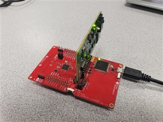
Despite those changes, my computer still won't interface with the microcontroller. I am programming the chip using JTAG and using the Launchxl-CC2640R2 jumpstart board. I can program the chip on the jumpstart board fine, but when I plug in my PCB it has an interface error. Is there someone that could verify that I am following the microcontroller specifications correctly and possibly give some pointers as to what might be wrong? The box in question is in the rev6.pdf, in the box labeled "PCB Specs".

Thanks in advance,

Jarom Christensen

rev6board_traces.pdfrev6.pdf

  • Jarom,

    I am not entirely sure I understand the problem. What exactly do you mean with "my computer still won't interface with the microcontroller"? Do you mean communicating via a  UART interface or via JTAG? Also, what do you mean by "jumpstart board"? 

    I glanced at your design and did not see anything specifically troubling about the cJTAG connections (which I believe is the root of the issues). However, as you mentioned, there might have been issues with the footprint and assembly which are difficult for me to see.

    In any case, I see that your design has several deviations from our reference designs, mostly in the PCB. In this case, I strongly recommend you to look at the documents below for our recommended guidelines, which also references the design files of our development boards (you will want to look at the LAUNCHXL-CC2640R2 design). 

    CC13xx/CC26xx Hardware Configuration and PCB Design Considerations

    Crystal Oscillator and Crystal Selection for the CC26xx and CC13xx Wireless MCUs (Rev. I)

    Hope this helps,

    Rafael

  • Rafael,

    Thanks for the reply! So, I followed both of those when I designed the PCB, and thought I followed things, though I could have missed things. What things are you seeing that I missed?

    I'll also describe my problem better. I think I was wrong in calling the board the "jumpstart" board. The text on the board says "LAUNCHXL-CC2640R2" and contains a CC2640R2F chip on one half, and the other half contains what I think is a programmer for the chip. There are pins that can be jumped across to program the embedded CC2640R2F, or another board can be plugged into those pins to be programmed, which is what I am doing. I am including a picture to make it more clear. I connect my board to the launchpad board, which I then plug into my computer via USB. I have tried this in Code Composer and the online programmer provided by TI, and I get an error:

    Error connecting to the target:
    (Error -242 @ 0x0)
    A router subpath could not be accessed.
    The board configuration file is probably incorrect.
    (Emulation package 9.6.0.00172)

    I've tried it on different machines and different ways and get the same error, and I'm assuming it's a hardware error. Have you seen this before?

    Thanks,

    Jarom

  • Hi Jarom,

    Thanks for sending the details of your setup. Indeed it improves clarity.

    The Error -242 is not uncommon and can be triggered by several root causes. Please check them in the Debugging JTAG page at: (search for the error number)

    https://software-dl.ti.com/ccs/esd/documents/ccs_debugging_jtag_connectivity_issues.html

    From the information provided it seems that a connector on the RF path was not designed (important for conducted tests) or ground planes on the RF parts or the decoupling capacitors' current return paths (sections 4.2, 4.6, 4.7 of the SWRA640 document) are a few examples.

    Best regards,

    Rafael

  • Rafael,

    I did some software and programming debugging and I don't think it's a software problem. The board I've shown you pictures of is revision 2 of this particular project, so I've been able to test with revision 1, which has the exact same microcontroller, just a different board layout. Even after swapping the microcontrollers between rev 2 and rev 1, we could still program rev 1 and couldn't program rev 2.

    Thank you for pointing out those sections to me. I have some questions about those because I thought I followed them, but I realize I may not fully understand the documentation. Let me tell you how I think the board follows the specifications, and you can correct me where I'm wrong.

    Section 4.2: I didn't follow the design mentioned in this section. However, that's because I decided to use differential operation, which is detailed in section 2.1. I didn't include the red wires because I believe I am using the internal bias, as the document says. I could be wrong about that though. The one problem I noticed as I went over it again was that I accidentally switched the positive and negative RF pins. Could that be enough of a problem to not allow programming?

    Section 4.6: I have all the decoupling capacitors from the power lines to the bottom ground plane, which connects to the EGP though vias below the EGP.

    Section 4.7: This one I definitely didn't understand fully when I designed the board. I attempted to conform to section 11.2, which is why it looks how it does. How should I have done this?

    Thanks so much for your help!

    Jarom

  • According to your schematic there does not seem to be a connection between VCC and VDDS. The extensive use of connect-by-name makes it pretty horrible to read so I may be overlooking something. 

    The layout is also pretty bad. If you are unsure about the guidelines in SWRA640 I would recommend looking at the reference design. Some of the worst issues:

    • No ground bias for the RF circuitry.
    • DCDC layout.
    • Is the blue dotted line ground plane? If so you need to clear it out from underneath the antenna.

    You should move as much signal routing to the top layer and reserve as much as possible of the bottom layer for a continuous ground plane.