This thread has been locked.

If you have a related question, please click the "Ask a related question" button in the top right corner. The newly created question will be automatically linked to this question.

CC2640R2F: Sensor Controller Studio 8bitTxRx SPI behavior Unexpected

Part Number: CC2640R2F
Other Parts Discussed in Thread: LAUNCHXL-CC2640R2

Hello,

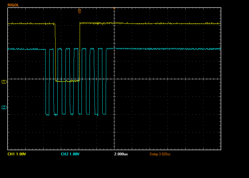
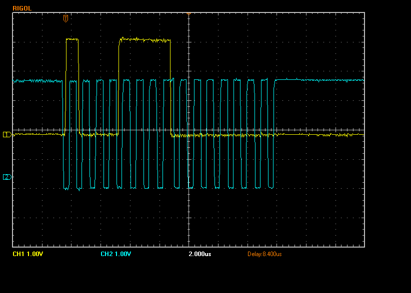
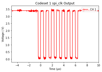
I am debugging an issue using sensor controller studio- two versions of the task function execution code, and the corresponding measured SPI_CLK waveforms

spiBegin(SPI_POL1_PHA1, AUXIO_SPI_CSN_ACCEL_CSN);
spiTxRx8bit(SPI_POL1_PHA1, (bitMsk_RD + addr_WHO_AM_I); output.partID);
spiEnd(SPI_POL1_PHA1, AUXIO_SPI_CSN_ACCEL_CSN);

spiBegin(SPI_POL1_PHA1, AUXIO_SPI_CSN_ACCEL_CSN);
spiTx8bit(SPI_POL1_PHA1, (bitMsk_RD + addr_WHO_AM_I));
spiRx8bit(SPI_POL1_PHA1; output.partID);
spiEnd(SPI_POL1_PHA1, AUXIO_SPI_CSN_ACCEL_CSN);

The difference in the two codesets is if the TxRx is done in a one or two lines; as described in the SPI Data Transfer section of Sensor Controller Studio Help Viewer, I would expect this to produce the same number of clock pulses- However, the single line waveform does not match my understanding of how this function works.

The hardware is custom board with a sensor attached to the SPI bus. I have experienced an issue pointing to the XTAL (Using the RCOSC build of simple_peripherial allows bluetooth functionality), and possibly further assembly issues, however, I expect this is independent of possible hardware bugs. I'm using SCS 2.9.0.208

  • Hello Barrett,

    Here is a link to the SPI Data Transfer section of the Sensor Controller Studio v2.9.0 Documentation.  Your implementation appears to be correct.  Do you receive any SPI bytes for the first implementation in output.partID?  What is the behavior of the other SPI lines?  If it does not cause any issues then I would recommend continuing with the second implementation.

    Regards,
    Ryan

  • Hi Ryan,

    Currently on the board I'm debugging I measure a short between the data in, data out pins; I don't know if this is the expected electrical measurement within the part or if this can only be a short on the board. The oscilloscope measurement shows no activity on the data in/data out, however I can remeasure with plots.

    The single line implementation returns the written value as the read value, the two line implementation returns all zeros.

  • It would be worthwhile to test your board's activity against that of a LAUNCHXL-CC2640R2, as this would indicate whether the issue is related to hardware or software.

    Regards,
    Ryan

  • Hi Ryan,

    Good point. I can probe the launchpad easier this way, too. Running the same code, I can monitor the MOSI signal on channel 2:

    One Line Scope Plot:

    Two Line Scope Plot:

    The two line implementation writes the correct value of 8F for read bit (0x0080) logical and addr bit (0x000F).

  • Am I interpreting correctly that they MOSI is at a different default level depending on the implementation used (one-line vs two-line)?

    Regards,
    Ryan

  • Ryan,

    Yes, in the first case the default level is high, in the second it is default low

  • Are you able to reproduce these results on your bench?

  • I don't have the correct hardware so I am checking to determine if another TI representative can confirm your findings.  Meanwhile you should continue to use the two-line commands.

    Regards,
    Ryan

  • Hey Barrett,

    I have the hardware but am not familiar with Sensor Controller Studio, can you send me a minimal set of projects to reproduce this behavior?

  • Hi Ammar,

    I've attached the .scp file as .txt. You will have to download, change the extension, and open in SCS. The main thing that I have setup is the IO mapping:

    In the plots above, I am measuring MOSI on DIO27 and CLK on DIO28.

    On the 5x5 part, I am using DIO9, DIO10, DIO11, and DIO12; This is my best guess at how the remapping is done for the different package sizes.

    The execution code is 5 lines, with the comment character "//" to toggle between the two cases

    <?xml version="1.0" encoding="UTF-8"?>
    <project name="CC1Acc SCS Test3 LPXL" version="2.9.0.208">
        <desc><![CDATA[]]></desc>
        <pattr name="Apply default power mode">0</pattr>
        <pattr name="Board">CC1A</pattr>
        <pattr name="Chip name">CC2640R2F</pattr>
        <pattr name="Chip package">QFN48 7x7 RGZ</pattr>
        <pattr name="Chip revision">-</pattr>
        <pattr name="Clock in active mode">0</pattr>
        <pattr name="Code prefix"></pattr>
        <pattr name="Default power mode">0</pattr>
        <pattr name="Operating system">TI Driver Porting Layer</pattr>
        <pattr name="Output directory">./</pattr>
        <pattr name="RTC tick interval (16.16 format)">2000</pattr>
        <pattr name="Run-time logging UART RX pin"></pattr>
        <pattr name="Run-time logging UART TX pin"></pattr>
        <task name="CC1AccInq">
            <desc><![CDATA[Task opens SPI connection to accellerometer and requests ID]]></desc>
            <tattr name="addr_STATUS_REG" type="expr_hex" content="const" scope="task" min="0" max="65535">0x27</tattr>
            <tattr name="addr_SelfTest" desc="self test register" type="expr_hex" content="const" scope="task" min="0" max="65535">0x0000</tattr>
            <tattr name="addr_Temp_Config" desc="Temp Config Register Address" type="expr_hex" content="const" scope="task" min="0" max="65535">0x1F</tattr>
            <tattr name="addr_WHO_AM_I" type="expr_hex" content="const" scope="task" min="0" max="65535">0x0F</tattr>
            <tattr name="bitMsk_RD" type="expr_hex" content="const" scope="task" min="0" max="65535">0x0080</tattr>
            <tattr name="input.addrInquire" type="expr_hex" content="struct" scope="task" min="0" max="65535">addr_WHO_AM_I</tattr>
            <tattr name="input.addrST" type="expr_hex" content="struct" scope="task" min="0" max="65535">addr_SelfTest</tattr>
            <tattr name="input.addrStatus" type="expr_hex" content="struct" scope="task" min="0" max="65535">addr_STATUS_REG</tattr>
            <tattr name="input.addrTempConfig" type="expr_hex" content="struct" scope="task" min="0" max="65535">addr_Temp_Config</tattr>
            <tattr name="output.STout" type="expr_hex" content="struct" scope="task" min="0" max="65535">0</tattr>
            <tattr name="output.partID" type="expr_hex" content="struct" scope="task" min="0" max="65535">0</tattr>
            <tattr name="output.partStatus" type="expr_hex" content="struct" scope="task" min="0" max="65535">0x00</tattr>
            <tattr name="output.tempReg" type="expr_hex" content="struct" scope="task" min="0" max="65535">0000</tattr>
            <resource_ref name="ADC" enabled="0"/>
            <resource_ref name="AON Domain Functionality" enabled="0"/>
            <resource_ref name="Accumulator-Based Math" enabled="0"/>
            <resource_ref name="Analog Open-Drain Pins" enabled="0"/>
            <resource_ref name="Analog Open-Source Pins" enabled="0"/>
            <resource_ref name="Analog Pins" enabled="0"/>
            <resource_ref name="COMPA" enabled="0"/>
            <resource_ref name="COMPA Event Trigger" enabled="0"/>
            <resource_ref name="COMPB" enabled="0"/>
            <resource_ref name="COMPB Event Trigger" enabled="0"/>
            <resource_ref name="Delay Insertion" enabled="0"/>
            <resource_ref name="Differential Output Pins" enabled="0"/>
            <resource_ref name="Digital Input Pins" enabled="0"/>
            <resource_ref name="Digital Open-Drain Pins" enabled="0"/>
            <resource_ref name="Digital Open-Source Pins" enabled="0"/>
            <resource_ref name="Digital Output Pins" enabled="0"/>
            <resource_ref name="Dynamic Power Control" enabled="0"/>
            <resource_ref name="GPIO Event Trigger" enabled="0"/>
            <resource_ref name="I2C Master" enabled="0">
                <rattr name="SCL frequency">0</rattr>
                <rattr name="SCL stretch timeout">1</rattr>
                <io_usage>
                    <uattr name="Output drive strength">1</uattr>
                    <uattr name="SCL pin/0000"></uattr>
                    <uattr name="SDA pin/0000"></uattr>
                </io_usage>
            </resource_ref>
            <resource_ref name="ISRC" enabled="0"/>
            <resource_ref name="LCD Controller" enabled="0">
                <rattr name="Waveform state count">8</rattr>
                <io_usage>
                    <uattr name="Output drive strength">0</uattr>
                    <uattr name="Pin count">20</uattr>
                    <uattr name="Pin/0000"></uattr>
                    <uattr name="Pin/0001"></uattr>
                    <uattr name="Pin/0002"></uattr>
                    <uattr name="Pin/0003"></uattr>
                    <uattr name="Pin/0004"></uattr>
                    <uattr name="Pin/0005"></uattr>
                    <uattr name="Pin/0006"></uattr>
                    <uattr name="Pin/0007"></uattr>
                    <uattr name="Pin/0008"></uattr>
                    <uattr name="Pin/0009"></uattr>
                    <uattr name="Pin/0010"></uattr>
                    <uattr name="Pin/0011"></uattr>
                    <uattr name="Pin/0012"></uattr>
                    <uattr name="Pin/0013"></uattr>
                    <uattr name="Pin/0014"></uattr>
                    <uattr name="Pin/0015"></uattr>
                    <uattr name="Pin/0016"></uattr>
                    <uattr name="Pin/0017"></uattr>
                    <uattr name="Pin/0018"></uattr>
                    <uattr name="Pin/0019"></uattr>
                    <uattr name="Pin/0020"></uattr>
                    <uattr name="Pin/0021"></uattr>
                    <uattr name="Pin/0022"></uattr>
                    <uattr name="Pin/0023"></uattr>
                    <uattr name="Pin/0024"></uattr>
                    <uattr name="Pin/0025"></uattr>
                    <uattr name="Pin/0026"></uattr>
                    <uattr name="Pin/0027"></uattr>
                    <uattr name="Pin/0028"></uattr>
                    <uattr name="Pin/0029"></uattr>
                    <uattr name="Pin/0030"></uattr>
                    <uattr name="Pin/0031"></uattr>
                </io_usage>
            </resource_ref>
            <resource_ref name="Math and Logic" enabled="0"/>
            <resource_ref name="Multi-Buffered Output Data Exchange" enabled="0">
                <rattr name="Buffer count">2</rattr>
                <rattr name="Indicate overflow at buffer check">1</rattr>
                <rattr name="Indicate overflow at buffer switch">0</rattr>
                <rattr name="Prevent overflow at buffer switch">1</rattr>
            </resource_ref>
            <resource_ref name="Peripheral Sharing" enabled="0"/>
            <resource_ref name="Pulse Counter" enabled="0"/>
            <resource_ref name="RTC Multi-Event Capture" enabled="0"/>
            <resource_ref name="RTC-Based Execution Scheduling" enabled="0"/>
            <resource_ref name="Reference DAC" enabled="0"/>
            <resource_ref name="Run-Time Logging" enabled="0"/>
            <resource_ref name="SPI Chip Select" enabled="1">
                <io_usage name="ACCEL_CSN" label="Accelerometer Chip Select">
                    <uattr name="CSN configuration when idle">0</uattr>
                    <uattr name="CSN pin/0000">DIO25</uattr>
                </io_usage>
            </resource_ref>
            <resource_ref name="SPI Data Transfer" enabled="1">
                <rattr name="Bit rate">1</rattr>
                <rattr name="MISO configuration when inactive">-1</rattr>
                <rattr name="MOSI configuration on initialization">1</rattr>
                <rattr name="MOSI configuration on uninitialization">-1</rattr>
                <rattr name="SCLK configuration on initialization">1</rattr>
                <rattr name="SCLK configuration on uninitialization">1</rattr>
                <io_usage>
                    <uattr name="MISO pin/0000">DIO26</uattr>
                    <uattr name="MOSI pin/0000">DIO27</uattr>
                    <uattr name="SCLK pin/0000">DIO28</uattr>
                </io_usage>
            </resource_ref>
            <resource_ref name="Signal Observation" enabled="0"/>
            <resource_ref name="System CPU Alert" enabled="0"/>
            <resource_ref name="System Event Trigger" enabled="0"/>
            <resource_ref name="TDC" enabled="0"/>
            <resource_ref name="Timer 0" enabled="0"/>
            <resource_ref name="Timer 0 Event Trigger" enabled="0"/>
            <resource_ref name="Timer 1" enabled="0"/>
            <resource_ref name="Timer 1 Event Trigger" enabled="0"/>
            <resource_ref name="Timer 2" enabled="0"/>
            <resource_ref name="Timer 2 Event Trigger" enabled="0"/>
            <resource_ref name="UART Emulator" enabled="0">
                <rattr name="RX buffer size">64</rattr>
                <rattr name="Required idle period before enabling RX">11</rattr>
                <rattr name="TX buffer size">64</rattr>
                <io_usage>
                    <uattr name="RX pin/0000"></uattr>
                    <uattr name="TX pin/0000"></uattr>
                </io_usage>
            </resource_ref>
            <sccode name="event0" init_power_mode="0"><![CDATA[]]></sccode>
            <sccode name="event1" init_power_mode="0"><![CDATA[]]></sccode>
            <sccode name="event2" init_power_mode="0"><![CDATA[]]></sccode>
            <sccode name="event3" init_power_mode="0"><![CDATA[]]></sccode>
            <sccode name="execute" init_power_mode="0"><![CDATA[spiBegin(SPI_POL1_PHA1, AUXIO_SPI_CSN_ACCEL_CSN);
    //spiTxRx8bit(SPI_POL1_PHA1, (bitMsk_RD + addr_WHO_AM_I); output.partID);
    spiTx8bit(SPI_POL1_PHA1, (bitMsk_RD + addr_WHO_AM_I));
    spiRx8bit(SPI_POL1_PHA1; output.partID);
    spiEnd(SPI_POL1_PHA1, AUXIO_SPI_CSN_ACCEL_CSN);]]></sccode>
            <sccode name="initialize" init_power_mode="0"><![CDATA[//if pol0pha0:
    
    //spiBegin(SPI_POL0_PHA0, AUXIO_SPI_CSN_ACCEL_CSN);
    //spiTxRx8bit(SPI_POL0_PHA0, 0x8F; output.partID);
    //spiEnd(SPI_POL0_PHA0, AUXIO_SPI_CSN_ACCEL_CSN);


    //if pol1pha1
    //spiBegin(SPI_POL1_PHA1, AUXIO_SPI_CSN_ACCEL_CSN);
    //spiTxRx8bit(SPI_POL1_PHA1, 0x8F; output.partID);
    //spiEnd(SPI_POL1_PHA1, AUXIO_SPI_CSN_ACCEL_CSN);


    //Set up SPI parameters based on SCS Help
    //SPI_POL0_PHA0    First edge of SCLK is rising, MOSI/MISO sampled at first edge of SCLK
    //SPI_POL0_PHA1    First edge of SCLK is rising, MOSI/MISO propagated at first edge of SCLK
    //SPI_POL1_PHA0    First edge of SCLK is falling, MOSI/MISO sampled at first edge of SCLK
    //SPI_POL1_PHA1    First edge of SCLK is falling, MOSI/MISO propagated at first edge of SCLK]]></sccode>
            <sccode name="terminate" init_power_mode="0"><![CDATA[//Close SPI connection
    //spiEnd(SPI_POL1_PHA1, AUXIO_SPI_CSN_ACCEL_CSN);]]></sccode>
            <event_trigger active_count="1">0,1,2,3</event_trigger>
            <tt_iter>wait_10ms,run_execute</tt_iter>
            <tt_struct>output.partID</tt_struct>
            <rtl_struct></rtl_struct>
            <rtl_task_sel en="1" struct_log_list="output"/>
        </task>
    </project>
    

  • Thanks Barrett. Let me look into this and I will get back to you.