This thread has been locked.

If you have a related question, please click the "Ask a related question" button in the top right corner. The newly created question will be automatically linked to this question.

CC2651R3: Not able to initialize the flash and also verify the Flash info

Expert 1760 points
Part Number: CC2651R3
Other Parts Discussed in Thread: SYSCONFIG

Hi team,

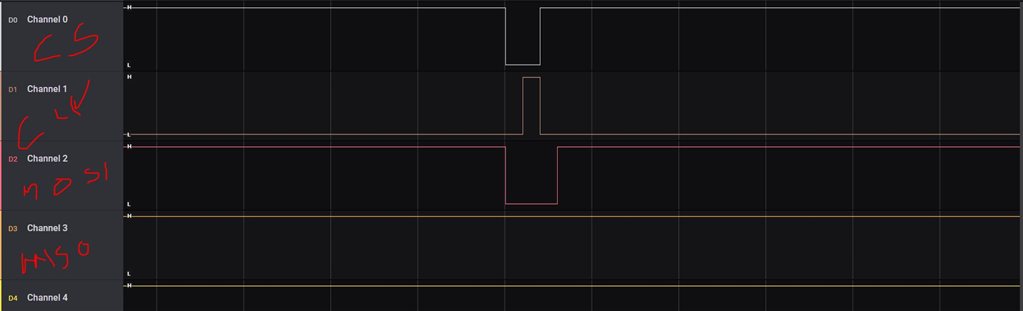
I'm working on CC2651R3 mcu with ble sdk 5.40. The external flash used is W25Q16JV.

In our project we are using External flash for OTA purpose. 

Currently i'm trying to verify the working of External flash, so used the available driver file ExtFlash.c and ExtFlash.h. I tried to call the functions already available as:

 flashSuccess = ExtFlash_open();
  ExtFlashInfo_t *flashInfo = ExtFlash_info();
 
But the ExtFlash is not initializing, and when I debugged I understood that the ExtFlash_readInfo() is reading 0xFF instead of Manufacture and Device ID.
 
May I know what could be the reason for this?
Thanks.
Note; I have also raised a case in TI support with case #CS1301296
  • Hi,

    The files ExtFlash.c and ExtFlash.h have been written and tested with certain external flash devices, and it looks like the specific flash used in this case is not part of the list (see flashInfo[] in ExtFlash.c).

    I would recommend to use a logic analyzer and compare the signals received by the flash to the ones stated in its datasheet in order to confirm this. Please use an actual logic analyzer (rather than an oscilloscope) so you can interpret the SPI signals easily.

    I hope this will help,

    Best regards,

  • [deleted]
  • Thanks Clement for your immediate response.

    Yes, I understood. We are using a 16Mbit Windbond flash. Here i attach the read and write signals, when writing and reading the flash info (as per ExtFlash.c) taken using Salae logic analyzer.

    Write - 

    const uint8_t wbuf[] = { BLS_CODE_MDID, 0xFF, 0xFF, 0x00 };

    extFlashSelect();

    int ret = Spi_write(wbuf, sizeof(wbuf));

    Read 

    ret = Spi_read(infoBuf, sizeof(infoBuf));

    CS and CLK lines are tapped on the PCB. MOSI and MISO lines are just connected to different pins (for testing) and not actually tapped into PCB. So please ignore the MISO lines (not supposed to get any data).

    Could you please clarify me if this is an expected behavioiur, "How does the CS pull high before completing the Write operation (as observed in figure 1) ? "

    From my understanding and based on the windbond flash datasheet, this is incorrect.

  • Write 4bytes (0x90,0xFF,0xFF,0x00) ---  (sampling rate increased to 8 Ms/s). MOSI and MISO not connected.

    Read (Manufacture and Device ID) - (sampling rate increased to 8 Ms/s). MOSI and MISO not connected.

  • Hi,

    Thank you for sharing these results.

    I would recommend to run the tests with all the signals connected to the device you are driving - otherwise the waveform will be altered. You can review our debugging guide for more information.

    In parallel, I have looked into the datasheet of the W25Q16JV flash.

    - "SPI bus operation Mode 0 (0,0) and 3 (1,1) are supported." ==> seems correct (SPI_POL0_PHA0)

    - "Instructions are initiated with the falling edge of Chip Select (/CS)." ==> seems correct on your plots

    - Looking at section §9.3.8 "Read Manufacturer / Device ID (90h)", I see a small inconsistency with the commands you are sending. According to the doc, the command should be (0x90,0x00,0x00,0x00) - I agree, this is not what was mentioned in §9.1.2

    Best regards,

  • Looking at section §9.3.8 "Read Manufacturer / Device ID (90h)", I see a small inconsistency with the commands you are sending. According to the doc, the command should be (0x90,0x00,0x00,0x00) - I agree, this is not what was mentioned in §9.1.2

    I think it should be OK since it is mentioned dummy bytes, instead of specifically 0x90, 0x00, 0x00, 0x00. Right ?

    But I tried using the the command 0x90,0x00,0x00,0x00, and still it reads 0xFF, 0xFF (2bytes) as Manufacture/Device ID.

    One more thing fyi, I'm using the ExtFlash.c files from \\ti\simplelink_cc13xx_cc26xx_sdk_5_40_00_40\source\ti\common\extflash . Is this the correct file to start with to test if the interface and the chip is working ?

    Note - We use external flash for OAD. So before starting with OAD we need to verify the SPI interface working.

  • Hi,

    You can use the spimaster example (<SDK>\examples\rtos\CC26X2R1_LAUNCHXL\drivers\spimaster) to reduce the complexity (and the overhead). But I don't expect much differences.

    In order to get this issue moved forward, I recommend you collect the wave forms with all the signals properly connected to the W25Q16JV flash and send these to the team supporting this part. 

    Thank you for your comprehension.

    Best regards,

  • As asked, please find the waveforms with all signals (SCLK, CS, MISO, MOSI):

    Please find the Instruction sent for reading Manufacture/Device ID, but while Reading MISO line gives 0xFF instead of actual data.

    Flash Write :

    FFlash Read:

    :

  • Hi,

    Thank you for sharing.

    Do you see any activity happening on the "MISO" line? (here it looks like the MISO line is always "high").

    At the moment, I suspect a hardware issue may actually happen. I mean, from the software point off view, we cannot fix much - the SPI receives 0xFF and reports 0xFF, so from this point of view everything is "working".

    The next steps I suggest are:

    - verify if the MISO line can be properly driven by the external flash. One approach could be to try to send other commands to the flash and see if the line toggles.

    - if the previous is not successful, consider to perform a hardware review. To me, the most efficient would be to have the inputs from the W25Q16JV flash support team. You can also request a design review from TI (see https://www.ti.com/tool/SIMPLELINK-2-4GHZ-DESIGN-REVIEWS).

    I hope this will help.

    I am now closing this thread as the issue is probably not at the software level. Please consider opening a new thread is additional support is needed.

    Best regards,

    Clement

  • Hi Clement,

    I have tried with the bim_oad_offchip no-rtos example from SDk5.40. 

    Modified the bsp.h to configure the pins as per our hardware.

    Executed the below operations and it works:

    if (extFlashOpen()){

    extFlashErase(0,sizeof(buffer));
    extFlashRead(100, sizeof(buffer), buffer);
    extFlashWrite(0, sizeof(init_data), init_data);

    extFlashRead(0, sizeof(buffer), buffer);

    }

    We are able to erase, read and write. So i don't doubt my hardware desing now. 

    My project is based on rtos, and when i use rtos example the SPI is not responding. May I know what I'm doing wrong?

    Thanks in advance.

  • Hi,

    Thank you for sharing this additional element.

    Assuming you get the external flash working on certain conditions, we can spot the differences between the working and the non-working case.

    - Could you please verify whether the signals sent by the CC2651R3 are identical or slightly different in the two cases?

    - Can you check if the SPI configuration is identical in both cases?

    - Can you check if in the nortos case you manage to read Manufacturer / Device ID?

    Best regards,

  •  

    Can you check if in the nortos case you manage to read Manufacturer / Device ID?

    Yes, I'am able to read Manufacture/Device ID.

    Can you check if the SPI configuration is identical in both cases?

    // Board external flash defines
    #define BSP_IOID_FLASH_CS IOID_17           -> IOCPinTypeGpioOutput(BSP_IOID_FLASH_CS);


    #define BSP_SPI_MOSI IOID_8
    #define BSP_SPI_MISO IOID_9
    #define BSP_SPI_CLK_FLASH IOID_16

    MOSI, MISO, CLK                             -> ROM_IOCPinTypeSsiMaster(BLS_SPI_BASE, BSP_SPI_MISO, BSP_SPI_MOSI, IOID_UNUSED /* csn */, clkPin);

    The configuration in no-rtos example is done as above. In bsp.h file I just changed the pin number. I have no idea how internally it is configured.

    Could you please verify whether the signals sent by the CC2651R3 are identical or slightly different in the two cases?

    Please find below the Writea and Read Manufacture ID together with SlaveSelect/ChipSelect line pulled low completely till end of both operation.

    Write 90H followed by FFh,FFh,00h (dummy bytes) for reading Manufacture/Device ID:

    Read Manufacture/Device ID:

  • Hi,

    May I kindly ask you to specify whether the traces you have shared in the previous message are taken from the working or the non-working case? Compared to the traces you have shared before, I see a difference on the CS line, but, at the same time, I still see the Manufacture/Device ID value read to be 0xFF.

    In the mean time, I have also reviewed the configuration of the SPI for you. To do so, I started from ext_flash.c (noRTOS) and ExtFlash.c (RTOS).

    - both configuration use the same bitrate (4000000)

    - both configuration use the same SPI mode (SPI mode Polarity 0 Phase 0)

    - both configuration use the same data size (8)

    - both configuration use the same mode (master)

    - the only difference is on the handling of the CS line. For the noRTOS code, the CS line is driven as a GPIO, i.e. basically lowered before the first transfer and set high after it. On the RTOS code, the CS line is handled by the SPI hardware, i.e. with the possibility to set it high between the bytes.

    In the end, to repeat myself, I would recommend to review the W25Q16JV flash datasheet and/or contact the team supporting this part to see if the behavior of the CS line could cause the erroneous values transferred.
    Alternatively, you may want to try to mimic the behavior of the CS observed with the noRTOS code. A pretty easy test could be to basically route the CS signal provided by the CC2651R3 to an unused pin, and basically connect the CS pin of the W25Q16JV flash to the ground.

    I hope this will help,

    Best regards,

  • Hi Clement,

    Thanks for  detailed explanation.

    1. 

    May I kindly ask you to specify whether the traces you have shared in the previous message are taken from the working or the non-working case?

         The traces are from working case, since I'm able to read the Manufacture/Device ID. I too wonder why the MISO line is still shows 0xFF.

    2. You are right. The difference is with the CS line, as I already mentioned "CS line is pulled LOW before starting operation and remains LOW till the entire           byte array (all 4 bytes - 0x90 ,0xFF, 0xFF, 0x00) is written into flash" which is expected. 

         But when using the RTOS code, after every byte is written (say 0x90 is written) the CS line is pulled HIGH which is not expected.

    3. I will contact the Winbond team.

    4. thanks for the mimic option, ill try that meanwhile.

  • Hi,

    I'll wait on your feedback. Please keep us posted!

    Best regards,

  • We just need to connect the configure an unused pin to CS line and ground the Flash CS pin right.

    When I try to mimic as mentioned, the Flash is not coming out of BUSY state to do further operations.

  • Hi Clement,

    I configured the DIO17 (the chipselect pin) to an unused GPIO for testing and the SPI CS is configured to a different GPIO. I could observe the same result as with no-rtos example. Able to read/write.

  • Hi,

    I configured the DIO17 (the chipselect pin) to an unused GPIO for testing and the SPI CS is configured to a different GPIO. I could observe the same result as with no-rtos example. Able to read/write.

    Great! You have probably found the root cause of the issue then (i.e. SPI CS line is not driven as expected by the W25Q16JV flash memory).

    The easiest path forward seems to reconfigure the SPI driver to use the "Three Pin" mode (should be doable using SysConfig).

    Then, one of the following options should be considered to drive the CS line.

    - Option 1: Basically ground the line - Advantage: no pin of the CC2651R3 is used | Drawback: only one SPI device can be interfaced

    - Option 2: Drive the CS line using a GPIO. Depending on your requirements, you could consider one of the following approach:

    1. Basically drive the line Low all the time - Advantages: easy to implement and low additional flash consumption
    2. Drive the line Low when the SPI module is opened - Advantages: still pretty easy to implement and low additional flash consumption
    3. Drive the line Low when SPI operations are performed - Advantage: the best option is you interface several SPI devices | Drawback: slightly more complex than the other suggestions + some timing issues may come into the picture

    I hope this will help,

    Best regards,