This thread has been locked.

If you have a related question, please click the "Ask a related question" button in the top right corner. The newly created question will be automatically linked to this question.

CC2652P7: Testing custom board CC2652P7 RF-BLE with SmartRF Studio7 - no TX signal on PA port, poor RX signal strength

Part Number: CC2652P7
Other Parts Discussed in Thread: TEST2, CC1352P, CC2652P, CC8520

Hello TI Team,

I am currently testing a prototype series of custom CC2652P7 boards with SmartRF Studio 7.

The board is correctly identified as CC2652P7_BLE-Device and seems to communicate correctly with SmartRF Studio.

I am using a LP-CC1352P7-4 board also connected to SmartRF Studio alternately in Continuous RX and TX mode to verify the corresponding operation of the custom CC2652P7 board.

Test1:

Continuous RX on CC2652P7, Continuous 5dBm TX on LP-CC1352P7-4

7.5mA supply current on CC2652P7, very poor RX RSSI -80dBm on CC2652P7

Test2:

Continuous TX on CC2652P7 5dBm, Continuous RX  on LP-CC1352P7-4

10mA supply current on CC2652P7, normal RX RSSI -100 --> -40dBm on LP-CC1352P7-4 (almost no signal)

Test3:

Continuous TX on CC2652P7 10dBm, Continuous RX  on LP-CC1352P7-4

8.9mA supply current on CC2652P7 (should be 19.5mA), RX RSSI -100 --> -95dBm on LP-CC1352P7-4

Test4:

Continuous TX on CC2652P7 20dBm, Continuous RX  on LP-CC1352P7-4

13.4mA supply current on CC2652P7 (should be >50mA), RX RSSI -100 --> -90dBm on LP-CC1352P7-4 (almost no signal)

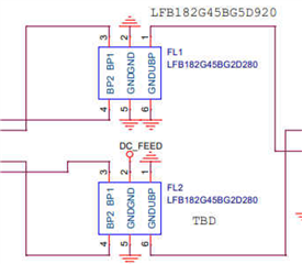
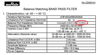
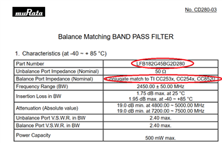
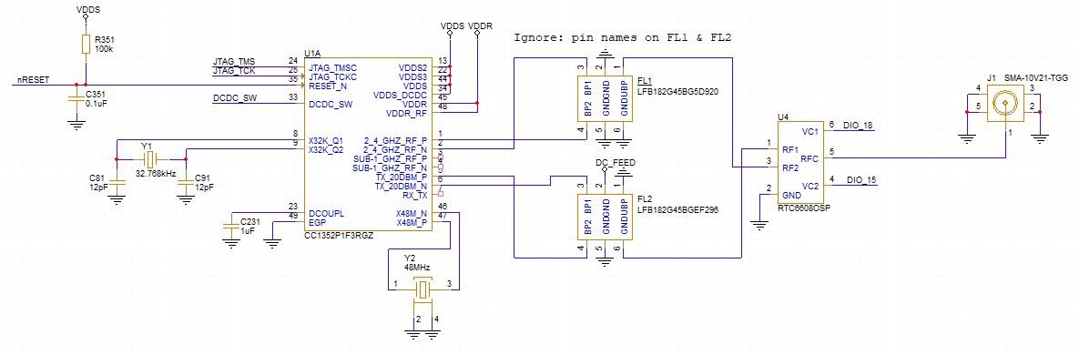
The RF network on the CC2652P7 is built according to "TI Application Note 2.4-GHz, 10-dBm PA IPC for CC26x2P and CC1352P" with 2 Murata IPCs  LFB182G45BG2D280 followed by a RF switch SKY13587-378LF.

During the test a payed particular attention to the correct setting of the RF switch when in RX, PA, and non PA mode.

Remark: on our custom board the 32kHz Crystal oscillator is not implemented (pin8,9 not connected).

From the behavior above in particular the unusual low supply current in 10/20dBm PA transmit mode could you eventually guess the origin of my problems?

All prototyping boards show exactly the same behavior so seems to be a systematic hardware error or configuration of the CC2652P7 by SmartRF Studio is not done properly.

Appreciating your help

Best regards

Christoph

  • Christoph,

    If I understood correctly all the test scenarios described above, it gives me the impression the connection between the two boards is not reliable or is broken in some way. To verify this, you could attach a spectrum analyzer to the output of your board and configure SmartRF to send an unmodulated carrier to verify the power and any spectrum anomalities that might be happening. You could also use two Launchpads to verify cables and connections.

    As for any design aspects, I noticed the RF path of the schematics does not show any DC blocking capacitors. I know the Skyworks switch requires them (as shown on its datasheet), but I am not very familiar with the IPC part and its datasheet is unclear regarding this requirement. If the IPC has a DC path to ground, this would disrupt the bias of the output PA and thus cause not only problems in RX/TX but also skew the device's power consumption. 

    I also spotted two additional deviations from our reference designs.

    - The RX path is not biased - typically done by the RXTX pin applied to the RX RF_P pin as shown in our reference design for a similar board such as the LP-CC2651P3
    - The RF Switch DIO pin assignments (DIO15 and DIO18) differ from our standard assignments (DIO28 and DIO29), which might cause the switch to be disabled if used with our standard projects and code.

    Hope this helps,

    Rafael

  • Hello Rafael,

    Many thanks for your comprehensive and valuable feedback.

    In particular your remark regarding biasing caught my attention and I compared DC voltages on RF_P,N pins and TX_20DBM_P,N pins in different TX, RX condition with LP-CC1352P7-4.

    For LP-CC1352P7-4 I got:
    RX: RF_P,N ~30mV
    TX5dBm: RF_P,N 0.65V
    TX10dBm: TX_20DBM_P,N: 1.6V (always VDDR)

    On my custom board CC2652P7 with IPC LFB182G45BG2D280 I got:
    RX: RF_P,N ~1V (poor RX RSSI)
    TX5dBm: RF_P,N 0.65V (TX RSSI ok similar to LP-CC1352P7-4)
    TX10dBm: TX_20DBM_P,N: ~15mV (no signal)

    My test environment was again 2 x LP-CC1352P7-4, one with my custom board connected and both operated by SmartRF Studio 7 in parallel.

    InSmartRF Studio 7 "External Bias Differential RF" was selected which I inherited from the original LP-CC1352P7-4 configuration. When I changed this to "Internal Bias Differential RF" the RX performance of my custom board significantly improved. Bias also changed during RX from ~1V to ~300mV.
    With Power amplifier switched off the RX, TX performance in 5dBm mode was excellent, equal to LP-CC1352P7-4.
    Still with Power amplifier ON I got no TX signal on TX_20DBM_P,N and bias remained at ~1.5mV.

    Next I checked the IPC LFB182G45BG2D280 with an Ohm meter. It seems no Inductors are between both balanced ports and towards pin 2 which in the PA path connects to VDDR. DC blocking capacitors obviously are available against GND pins. Obviously the PA path requires external bias as shown in the schematic of LP-CC1352P7-4 and does not support any internal bias configuration.

    May I draw you attention to https://www.ti.com/lit/an/swra729/swra729.pdf "2.4-GHz, 10-dBm PA IPC for CC26x2P and CC1352P". This TI application note describes the use of IPC LFB182G45BG2D280 for CC2652P PA applications particularly when space is limited.
    My custom board is designed according to the schematic "Figure 1-3. CC2652P PA IPC EM Rev 1.0 Schematic" using IPC LFB182G45BG2D280 as proposed. So I expected it to work same as the design with discrete parts of LP-CC1352P7-4.

    Can you please advise if there are any modifications or particular RF settings required to make this design working in PA mode?

    Best regards

    Christoph

  • Christoph,

    When I changed this to "Internal Bias Differential RF" the RX performance of my custom board significantly improved.

    Sorry, I forgot that this is indeed the default configuration for our Launchpads including the one used in the schematics I shared above. In this case, the improvement in the +5 dBm path is expected.

    Still with Power amplifier ON I got no TX signal on TX_20DBM_P,N and bias remained at ~1.5mV.

    Thanks for highlighting the app note - sorry I missed it from your original post.

    Indeed the blocking capacitors are not needed but the 1.5 mV of PA bias is indeed abnormal. The IPC should be feeding the RF_P with VDDS for +20 dBm operation or VDDR for +10 dBm operation. This is selected by the resistors R6/R7 shown in the schematics I shared above and is shown in Figure 1-2 of the app note (for +10 dBm). I wonder if it might have been damaged, but it would be a rare occurrence in all the boards of your lot.

    To circumvent the different RF switch DIO assignments and get an output on the +20 dBm RF path, you have to set these pins in SmartRF Studio. Op-en the Device Control Panel for the CC2652P7_BLE-Device, then enable the high output power PA and then go to menu Settings --> Custom Target Configuration. You should see the I/O signals for both the Tx and Rx paths

    I will try to gather some measurements on a board here and report back any findings.

    Regards,

    Rafael

  • Hello Rafael,

    Just to ensure common understanding:

    When I mention "custom hardware" I am talking about our custom board. This is connected to a LP-CC1352P7-4 launchpad for debugging. The local MCU on the launchpad is disabled. With SmartRF studio I am connected in parallel to this and a second LP-CC1352P7-4 which I use as reference for testing RX and TX mode of the custom board.
    On LP-CC1352P7-4 the default front end setting is "External Bias Differential RF" which at first I was using on my custom board as well.
    When I changed front end setting of the custom board to "Internal Bias Differential RF" RX RSSI increased from poor -80dBm to -40dBm.
    In our custom design according to Application note https://www.ti.com/lit/an/swra729/swra729.pdf Inductors L11, L12 and L52, L53 on the PA path are missing. This is the main difference to the LP-CC1352P7-4 schematics above.
    The setting "External Bias Differential RF" seems to have no effect on the PA path.
    LFB182G45BG2D280 seems to have no inductors inside so in the Application note design there seems to be no DC connection of the RF pins either to VDDR or VDDS or RX_TX.

    I do not believe that IPC LFB182G45BG2D280 is broken. I tested on 3 different boards with exactly the same results but con do some more to verify.

    I am also fully aware of the DIO setting options in Smart RF Studio. I created a custom target setting the DIOs appropriately and verified there status by Oscilloscope during TX, RX. In this dialog I also changed the front end settings from external to internal which improved the RX sensitivity significantly.

    Maybe it comes all down to understanding the behavior of the bias in the App note configuration. Also it would be helpful to have some schematic about the internal parts of IPC LFB182G45BG2D280. Unfortunately I could not find anything specific on the Murata website. I hope for a clear statement if we can continue with the App note design and release it for the next bigger production lot of our sensors.


    Best regards

    Christoph

  • Christoph,

    When I mention "custom hardware" I am talking about our custom board.

    Thanks for the clarification; I suspected you were using half LaunchPad for debugging but it is good to be 100% sure.

    When I changed front end setting of the custom board to "Internal Bias Differential RF" RX RSSI increased from poor -80dBm to -40dBm.

    Indeed that is expected. The +5 dBm path uses the internal bias since you followed the design shown in the app note.

    The setting "External Bias Differential RF" seems to have no effect on the PA path.

    The PA path requires external bias - either from VDDS or VDDR depending on the output voltage. One thing I find odd about the application note is the fact it only mentions +10 dBm but not +20 dBm, despite the IPC datasheet mentions a maximum power of 500mW (~26 dBm).

    LFB182G45BG2D280 seems to have no inductors inside so in the Application note design there seems to be no DC connection of the RF pins either to VDDR or VDDS or RX_TX.

    That shouldn't be the case when looking at section 1.1.1 (Figure 1-2) of the application note, which talks about the equivalent circuit of the IPC. The IPC should have L52 as a low impedance DC path. Can you measure an unsoldered IPC device and see if it has continuity between pin 2 and 3/4?

    I measured the voltages on a regular LaunchPad and indeed the VDDS bias (for +20 dBm) is present at the RF_P terminal of the PA.

    I will try to source one of these IPCs and do some measurements.

    Hope this helps,

    Rafael

  • Hello Rafael,

    First of all many thanks about your detailed investigation work to help resolving my issues.

    In the App note schematic Figure 1-3 one detail caught my attention. There are 2 types of IPCs mentioned.

    LFB182G45BG5D920 is written on top and LFB182G45BG2D280 next to FL1,2.
    Murata datasheet dedicates LFB182G45BG5D920 to CC26xx and LFB182G45BG2D280 to CC253x, CC254x, CC8520.

    Which part actually should be used together with a CC2652P7 MCU?

    Unfortunately Murata does not reveal any internal structure of their IPCs so from the datasheet I cannot see if inductors are there or not.

    I measured already several of my IPCs there is no continuity between pin2,3,4. So maybe LFB182G45BG2D280 which I am using is the wrong part.
    I really would appreciate if you can source one of these parts to verify if the inductors are there or not.
    We got our parts from Mouser. Unfortunately there is no label on the part to identify its type. It is not very likely but still possible that they might have shipped the wrong item.

    Best regards

    Christoph

  • Christoph,

    I was talking to one of the authors of the application note referenced above and he mentioned the figure has the wrong part numbers for the PA path.

    The IPC component for the PA is the LFB182G45BGEF296, which is qualified for the "P" devices:

    https://www.murata.com/en-global/products/productdetail?partno=LFB182G45BGEF296

    Naturally, with the correct part number I was able to find some discussions here on e2e about this via an internet search. Unfortunately I couldn't find stock at Mouser or Digikey, but I found it at Newark.

    I apologize for the confusion and delays this caused.

    Hope this helps,

    Rafael

  • Hello Rafael,

    LFB182G45BGEF296 seems to be very rare. Could you please post the link where you found the part at Newark.

    Best regards

    Christoph

  • Christoph,

    Indeed Newark also does not have this in stock - I was fooled by the equivalent return on my search.

    My suggestion is to contact Murata directly to request samples and a request for quote. They are usually very responsive.

    Best regards,

    Rafael

  • Christoph,

    Just FYI, we are closing the circle on this and updating the application note with the correct part numbers - a public version will be available in the near future. 

    The corrected figure 1-3 will be the following:

    Thank you for reporting this and please apologize for the error.

    Regards,

    Rafael

  • Hello Rafael,

    In your corrected figure DC blocking capacitors are missing as before. According to the datasheet RTC6608OSP these are required at RF1, RF2. I got a DC specification of LFB182G45BGEF296 and LFB182G45BG5D920 from Murata, For both types the unbalanced port has a DC path to GND.

    I am still struggling to get at least samples of the LFB182G45BGEF296 from Murata with little success yet. Maybe you can identify another IPC component which is available an also can satisfy the bias requirements of the PA port.

    Best regards

    Christoph

  • Christoph,

    For both types the unbalanced port has a DC path to GND.

    That is ok, as long as the balanced side does not have a DC path to GND.

    The reason for the DC blocking capacitors mentioned in the RTC6608OSP is that, in a normal application, the switch will be connected directly to the output of the PA. In this case, if the IPC already blocks DC, the PA bias will not be affected. 

    Please accept my friend request so I can share a contact at Murata that was sent to me. 

    Best regards,

    Rafael

  • Hello Rafael,

    Thank you for clarification. I did not know the details behind. Maybe this will help me reuse my prototype boards supposed I can source the LFB182G45BGEF296 somewhere.

    Appreciating your friendship request.

    Best regards

    Christoph