This thread has been locked.

If you have a related question, please click the "Ask a related question" button in the top right corner. The newly created question will be automatically linked to this question.

CC2340R5-Q1: SWD with J-LINK

Part Number: CC2340R5-Q1
Other Parts Discussed in Thread: CC2340R5, , LP-XDS110

Tool/software:

Dear team,

My customer is completing the PCBA assembly using our CC2340R52E0WRHBRQ1 to evaluate. 

1. Can the SWD interface of CC2340 be used with J-LINK programmer to program?
2. The customer plans to implement: standby after 10s of broadcasting→ wake up only through the RTC cycle of 60s → 10s of broadcasting → enter standby again.
 Is there a demo with similar functions for reference?
 How to enter standby? Is it calling the interface or does the hardware enter standby by itself when there is no broadcasting? Which resources need to be closed before entering standby?
 Is RTC enabled by default when powered on? Is initialization required? My customer said that he did not see any functions related to RTC. Where is the interrupt handler of RTC or how to set the handler? How to set the callback function of RTC interrupt?

Thanks for your warm support.

  • Hello,

    1. Can the SWD interface of CC2340 be used with J-LINK programmer to program?

    Yes, it should be able to be used.

     Is RTC enabled by default when powered on? Is initialization required? My customer said that he did not see any functions related to RTC. Where is the interrupt handler of RTC or how to set the handler? How to set the callback function of RTC interrupt?

    Please see our documentation here: Timers — SimpleLinkTm CC23xx SDK BLE5-Stack User's Guide 3.03.01.00 documentation

    And

    ClockP.h File Reference (ti.com)

     How to enter standby? Is it calling the interface or does the hardware enter standby by itself when there is no broadcasting? Which resources need to be closed before entering standby?

    The hardware will enter standby by itself. However, to ensure that the device goes into standby, all peripherals must be turned off (i.e. UART, ADCs, etc.).

    Best,

    Nima Behmanesh

  • Hi Nima,

    Thanks for your reply. Could you pls also answer these unmentioned questions?

    2. The customer plans to implement: standby after 10s of broadcasting→ wake up only through the RTC cycle of 60s → 10s of broadcasting → enter standby again.
     Is there a demo with similar functions for reference?
  • Hi Nima,

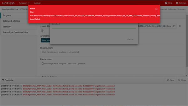
    We met an error during programming and we can't move on now. Could you pls help check if the program method is correct? If not please provide the correct method. Thanks for your urgent support!

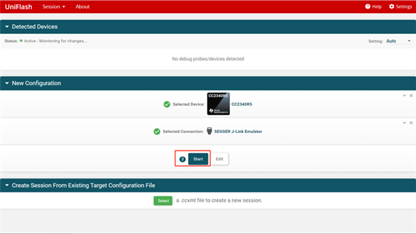
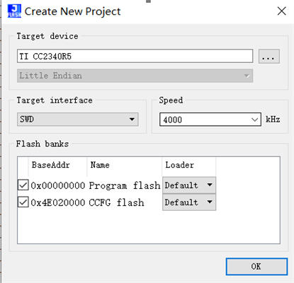
    1. Software settings on the PC:

    Select CC2340R5 chip, select J-LINK, click start

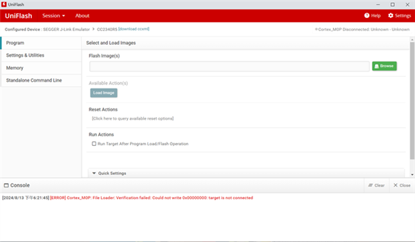
    Click start to go to the next screen

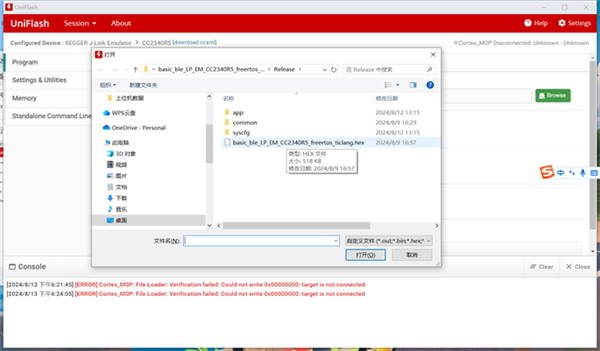
    Select File:

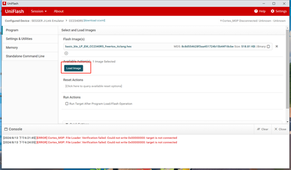
    Click load image

    Then an error is reported:

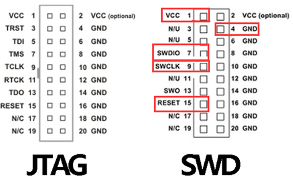
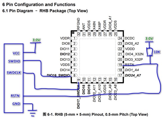
    2. JLINK connection method, using the SWD method of, the connection line sequence as shown below:

  • Hello,

    What pins are the lines from the Jlink device connected to the CC2340R5-Q1?

    Best,

    Nima Behmanesh

  • Hi Nima,

    Thanks for your reply. Addition to the question below, I also give them a LP-XDS110. It would be also helpful if you could tell me: Which pins does SWD use, and what software is used on the PC, and what are the programming steps?

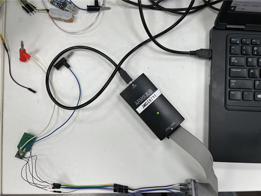
    Flying wire connection. 

    JLINK connection method, using the SWD method, the connection line sequence as shown below:

    Here are the details:

    When programming the CC2340R5 chip via J-FLASH, the following error occurs:
    0x0000 0000 program flash programming completed, 0x4E02 0000 CCFG flash programming failed. What is the reason for the failure of CCFG flash programming?

    Error log:

    - Start of flash programming

     - Programming range 0x00000000 - 0x00007FFF ( 16 Sectors, 32 KB)

     - Programming range 0x00008000 - 0x0000FFFF ( 16 Sectors, 32 KB)

     - Programming range 0x00010000 - 0x00017FFF ( 16 Sectors, 32 KB)

     - Programming range 0x00018000 - 0x0001FFFF ( 16 Sectors, 32 KB)

     - Programming range 0x00020000 - 0x00027FFF ( 16 Sectors, 32 KB)

     - Programming range 0x00028000 - 0x0002D7FF ( 11 Sectors, 22 KB)

     - End of flash programming

     - Flash programming performed for 1 range (186368 bytes)

     - 0x0000 - 0x2D7FF ( 91 Sectors, 182 KB)

     - Start of verifying flash

     - Using the native verify function of the flash algorithm

     - End of verifying flash

     - Start of restoring

     - End of restoring

     - Start of preparing flash programming

     - End of preparing flash programming

     - Start of determining dirty areas in flash cache

     - End of determining dirty areas

     - CPU speed could not be measured.

     - Start of erasing sectors

     - WARNING: Blank check not supported for this flash bank, skipped

     - Erasing range 0x4E020000 - 0x4E0207FF (  1 Sector, 2 KB)

     - End of erasing sectors

     - Start of flash programming

     - Programming range 0x4E020000 - 0x4E0207FF (  1 Sector, 2 KB)

     - ERROR: Programming failed @ address 0x4E020000 (Unspecified error #1)

     - ERROR: FLASH_RAMLESS: Failed to program target via J-Link

     - End of flash programming

     - ERROR: Program failed

     - Start of restoring

     - End of restoring

     - ERROR: Failed to auto program target

  • Hi Nima,

    My customer used LP-XDS110 and program successfully. Thanks