This thread has been locked.

If you have a related question, please click the "Ask a related question" button in the top right corner. The newly created question will be automatically linked to this question.

CC2674P10: Vpp value across the 48MHz quartz

Part Number: CC2674P10
Other Parts Discussed in Thread: CC1354P10, SYSCONFIG

Tool/software:

Hi, 

In https://www.ti.com/lit/an/swra495k/swra495k.pdf?ts=1728036718662&ref_url=https%253A%252F%252Fwww.google.com%252F 

Section 3.5 > "The CC13xx and CC26xx devices drive the crystal with a maximum 1.6 Vpp_differential for the 24/48-MHz"

> Drive level formula : DL = 2 x ESR (πf(CL + C0) Vpp)² ;

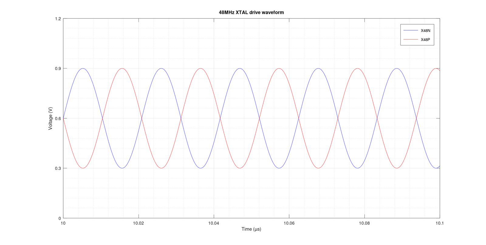
The CC1354P10_6 EVM uses the TZ3780AAAO44 with ESR = 30Ohms, CL = 7pF, Co = 3 pF, 48 MHz. The document says Vpp_diff = 1.6V so the DL = 349 µW > 200µW (max recommended) 

Would make more sense if the Vpp in the DS is the single-ended at one of the pins of the quartz. 

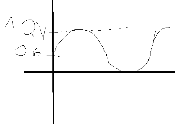
Finally, using the on-board ADC (section 5) I get the value ~430mV. 

  1. Vpp in the drive level formula is single-ended, correct ? 
  2. Is ~430 mV an excepted value for Vpp?

Thanks,

Geoffrey 

  • Geoffrey,

    Thanks for the inquiry. I can see from some other references the VPP value should instead be VRMS

    One of the references that develops the equation is at All about circuits:

    https://www.allaboutcircuits.com/technical-articles/measuring-drive-level-of-a-quartz-crystal/

    DL = ESR × ( π × f × ( CL + C0 ) )2 × ( VPP 2 ÷ 2 )

    In this case, if my calculations are correct the maximum drive level based on the XTAL used, the figures provided by its datasheet and the SWRA495 app note would place it somewhere around 87µW:

    DL = 30 × ( π × 48M × ( 7p + 3p ) )2 × ( 1.6 2 ÷ 2 )

    I will still consult with the authors of the app note in question, but that seems to be a more logical explanation for the discrepancy.

    The values of the VPP are not specified in the datasheet, but are within the limits mentioned in the SWRA495 app note, so they should be good.

    I will update this thread when I get additional information.

    Best regards,

    Rafael

  • Geoffrey,

    Reviewing my calculations, I assumed the drive voltage is sinusoidal. (edit, read below)  However, our devices issue a square wave and therefore the VRMS equals VP which is 0.5 × VPP

    In this case, the equation would become:

    DL = ESR × ( π × f × ( CL + C0 ) × VP )2

    And the result would be about 44 µW

    DL = 30 × ( π × 48M × ( 7p + 3p ) × 0.8 )2

    I will still get some additional details about the second question.

    Regards,

    Rafael

  • Hi Rafael, 

    Thank you for your feedback. 

    It makes more sense now, this detail should be specified in the document moving forward :) 

    In addition of the second question I have a third : 

    Is the voltage in the formula the Vrms at only one side of the quartz or should we consider the difference of the signals at the two pins of the quartz ? (they are in phase opposition) 

    Regards, 

    Geoffrey 

  • Hi Geoffrey,

    Is the voltage in the formula the Vrms at only one side of the quartz or should we consider the difference of the signals at the two pins of the quartz ? (they are in phase opposition) 

    The VPP and  VRMS values refer to the voltages applied across the XTAL, independently on the phase difference of the pins.

    Regards,

    Rafael

  • Hi Geoffrey,

    A few details and corrections from my previous replies.

    The drive voltage is in fact sinusoidal, so please use the calculations on my first post above. 

    Also, the 1.6 VPP mentioned in the application note is indeed applied to the crystal terminals via the X48_P and X48_N pins, but only for 3 µs during the initial startup. This higher level guarantees the XTAL can be started across the temperature range and accounts for part variability.

    After that, the steady state is a 600 mVPP sinusoidal wave with 0.6 V DC bias at each pin, but with a phase shift of 180° between them. The voltage levels and the phase shift are not exact as they are dependent on the normal part variability, temperature, etc. In practice, the value of ~400 mV your customer is reading off the ADC is well within the normal steady state operational margin. 

    Hopefully this clarifies the questions about the reliability of the XTAL. There are plans to add this information to the application note in a future release (a date is not yet set, though).

    Hope this helps,

    Rafael

  • Hi Rafael, 

    Thank you for your feedback. If I were to measure the voltage at X48_P I would measure the following correct ?  

    What are the Max and Min for Vpp ? 

    Regards, 

    Geoffrey 

  • Hi Geoffrey,

    The steady state waveform would be something like this:

    So, the Max and Min voltages would be 0.9 and 0.3 V, giving 0.6VPP

    (this image or some variation of it will become part of the application note in a future update).

    Cheers,

    Rafael

  • Hi Rafael,  

    Thank you,

    Are you sure about the Vpp ? 

    On our custom board we measure a Vpp ~1.1V (between GND and pin of the quartz). Can you double check on your EVM ? 

    Regards, 

    Geoffrey 

  • Geoffrey,

    I won't be able to measure this as I don't have an active probe available at this time - regular 10:1 probes can load the crystal excessively and cause distortions in the waveform. I can come back to this thread in the future if/when I get a setup going.

    Independently on what waveform I get, as I mentioned before there is quite some variation in the voltage levels due to various factors. The information I provided before are the typical values and waveforms.

    Regards,

    Rafael

  • Hi Rafael, 

    We would like an official confirmation for this topic. We measured Vpp ~1.1V at runtime, leading to a DL out of the recommended range, which still worries us. 

    • Have you found the right setup for the tests on EVMs ? 
    • Any explanation about why we measure 1.1V ? 

    Regards, 

    Geoffrey 

  • Geoffrey,

    Sorry for the delay; I didn't see your reply.

    The information provided before is our official stance on this, since this was provided by the design team.

    I couldn't get the proper setup but, even if I could, measuring a single board gives no significant statistical result that would prove one way or another.

    Also, as I mentioned before, the measurement technique might yield differences in the values obtained (probe techniques, probe capacitance, etc). Also, apart from device and temperature variances, did you also check the device settings? For example, you could try to experiment using different cap array values configured in sysconfig - not that I think they would influence the voltage swing significantly, but a very off value might cause unexpected effects.

    If you can provide further information and screen captures of your test setup and screens, that could be useful to try and debug this.

    Best regards,

    Rafael