Tool/software:
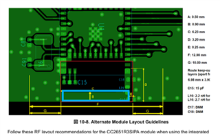
Regarding the RF layout, guideline 10.4.2 in the datasheet recommends an L1-2 interlayer thickness, 4 layers, and a dielectric constant, but since I cannot design according to these recommended values, I am proceeding with the design according to guideline 10.4.4.
When designing according to guideline 10.4.4
(1) Two values are listed for L16: 0.8mm and 1.6mm thickness, but how should I design if the board thickness is other than these?
Currently, I am considering a board thickness of 0.8mm or 1.0mm.
(2) Can I assume that the number of layers (interlayer thickness) has no effect?
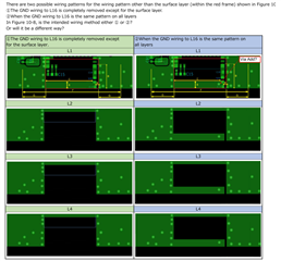
(3) In Figure 10-8, is it okay to punch out all layers except the surface layer within the red frame?
Or should I make the same pattern as the surface layer only on the GND side of L16 (blue frame in the attached figure)?