This thread has been locked.

If you have a related question, please click the "Ask a related question" button in the top right corner. The newly created question will be automatically linked to this question.

CC2340R5: Abnormal current draw

Part Number: CC2340R5

Tool/software:

Hi TI Team,

I am having some problems with my design using CC2340R52E0RKPR.

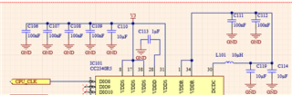
My design schematics are very close to the demoboard LP-EM-CC2340R5 schematics. Here is a picture of my design V3 power and DCDC schematics:

With an amp meter on my V3, in all cc2340R5 mode, I can see strange current peaks of 8 to 10 mA for about 1ms. These peaks have a period of 475ms. See the picture below :


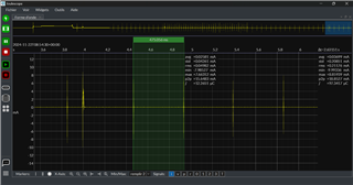
In my understanding it is caused by the two inductors of the DCDC charge, C119 and C114. When I remove one, the 475ms period decrease. Is it a normal operation of the CC2340R5?

Because these peaks increase my average consumption and I would like to make them disappear or decrease. What is the cause and what should I do? Do I need to adjust the DCDC components?

I have tried to follow this manual but without any changes:

https://software-dl.ti.com/simplelink/esd/simplelink_lowpower_f3_sdk/7.40.00.64/exports/docs/ble5stack/ble_user_guide/html/ble-stack-5.x/optimization-power-cc23xx.html

Thanks,

Best regards,

Titouan

  • Hi Titouan,

    What state is the device when you are running this test?

    To me it seems to be advertising every 475ms, and depending on your output power, if you take weighted average over the total time with time as the weight, a 1ms,10mA spike every 475ms seems reasonable.

    Best regards,

    Bun

  • Hi Bun,

    Thanks for the answer. The device is in Standby when I am running this test but i can see same peaks every 475ms in every state of the device.

    It's not advertising every 475ms , i verified it with a spectrum analyser.

    My application works with a small battery and need to be low consumption. The picture below shows the current draw zoomed, the left peak is the 10 mA peak every 475ms.

    Best regards,

    Titouan

  • Hi Titouan,

    If the device is in standby and no BLE events are happening, then these are recharge pulses which are inherent to DCDC. You can remove one of the 10uF capacitors as our reference design only requires 1 and see if you are ok with the performance.

    If you want to remove both 10uF, expect higher DCDC ripple currents and more frequency recharge pulses. I am expecting more overall current draw here.

    Best regards,

    Bun

  • Hi Bun,

    Ok thanks, that's what I was thinking.

    I think I can optimise the inductor and capacitor value of the DCDC, right?

    I think I can also optimise the consumption using the GLDO. Is it possible to chose/use the GLDO when the device is in standby and chose/use the DCDC when the device has BLE events? Can I dynamically choose between the GLDO and the DCDC?

    Best regards,

    Titouan

  • Hi Titouan,

    Toggling between DCDC and GLDO is not possible unless the driver code is rewritten to support it and these recharge pulses will still exist regardless of GLDO or DCDC

    Best regards,

    Bun