This thread has been locked.

If you have a related question, please click the "Ask a related question" button in the top right corner. The newly created question will be automatically linked to this question.

CC2640R2F: Internal DC-DC is not start-up

Part Number: CC2640R2F
Other Parts Discussed in Thread: CC2640, LP-XDS110ET, LAUNCHXL-CC2640R2, ENERGYTRACE

Tool/software:

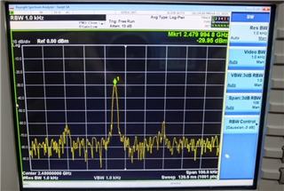
For our application, based on CC2640R2F chipset, design a BLE module, power supply use DC/DC converter mode, recently we found that small amount module are not working properly, when checking the hardware signal, we found that DCDC_SW pin has no square signal, it can measure 1.61V signal on DCDC_SW and the min voltage measured on VDDR is about 1.57V, both signal are measure via oscilloscope. we also measure the voltage of launchpad board, the voltage on VDDR is about 1.61V. 

so we are wondering:

  • in which case, the internal DC/DC will not start up, please not that the supply voltage on VDDS, VDDS2 and VDDS3 is nomal with 3.3V
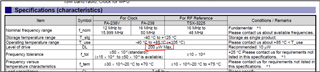
  • why the measured voltage on VDDR is 1.61 while according to spec and swra640 document, it should be 1.68V to 1.95V
  • Hi,

    The DCDC can be powered down in some low-power or shutdown states. Also, make sure the DCDC is enabled in your software.

    The thread below contains some additional details about these topics:

    https://e2e.ti.com/support/wireless-connectivity/bluetooth-group/bluetooth/f/bluetooth-forum/1163386/cc2640r2f-question-about-vddr-behavior

    Hope this helps,

    Rafael

  • When CC2640 starts, it will use global LDO as the power source firstly?

    can you share the details regarding DCDC enable in firmware?

    Currently when we found that the chipset is not started, the power consumption is about 7mA read from power supply instrument

  • Hi,

    When CC2640 starts, it will use global LDO as the power source firstly?

    Yes. For details, please check section 6.6.1 of the CC2640R2 Technical Reference Manual (SWCU117)

    can you share the details regarding DCDC enable in firmware?

    This is usually performed via the driverlib function SysCtrl_DCDC_VoltageConditionalControl(), which is included in all the example projects inside the file driverlib.lib and referenced by the file sys_ctrl.h. However, this is directly configured in the file ccfg.c of the example projects, as shown in the section 11.2 of the companion application note CC13xx/CC26xx Hardware Configuration and PCB Design Considerations (SWRA640)

    Currently when we found that the chipset is not started, the power consumption is about 7mA read from power supply instrument

    If there are no external peripherals or devices enabled, this level of current indicates the device might have its radio powered on (table 8-4 of the datasheet shows the various current consumption numbers of various states of the device.

    Hope this helps,

    Rafael

  • I ereased the chipset and found the current consumption is about 7~8mA, while for unormal module, the current consumption is similar, is there any possiblity that the chipset still stay in Ti boot rom and lead to current situation? is there any information regarding your boot room or how to verify?Thanks.

  • Hi,

    Since you erased the device, I assume you have it connected to a XDS110 Debug Probe, is that so? If so, your device should then have stable power and be running the ROM bootloader.

    The 7~8 mA of current would be normal if the device is in Active mode and the debug probe is connected to it (which powers up the Debug Subsystem of the device, adding a bit more to the current consumption).

    I would ask: how are you measuring the current? An averaging multimeter might show skewed measurements, especially if the processor has its radio turned on (there are spikes of current during transmission, for example).

    The application note below shows methods to measure the current consumption of the wireless connectivity devices.

    https://www.ti.com/lit/pdf/swra478

    Hope this helps,

    Rafael

  • I earase the chipset via J-Link, use power analyzer(Keysight N6705C) as power supply and read the current consumption from the display without J-Link connected to it.

    if SET_CCFG_BL_CONFIG_BOOTLOADER_ENABLE is defined as 0x00 in ccfg.c, would that ROM boot loader taken effect?

  • Hi,

    If you are using a custom board, make sure it does not have any other subsystems or peripherals that might be contributing to the higher current consumption - for example, external sensors or connections to external I2C or UART that could add to the overall leakage.

    Also, reviewing your original post I see that you are suspicious the DCDC is not operating correctly. I would thoroughly review your design following the directives of the app note SWRA640 mentioned in one of my previous posts. 

    Unfortunately I can't reproduce the increased current consumption you are seeing. The curves below show the measurements on a LAUNCHXL-CC2640R2 Launchpad using an Energytrace capable XDS110 debug probe (LP-XDS110ET or another Launchpad enabled for that). Notice the average current is around 5.6mA and the spikes are caused by the DCDC switching. The Flash memory is erased and the device was powered on just before this measurement. Also, the VDDR voltage measured on a simple True RMS portable voltmeter is 1.67V.

    The curves below show the measurements after the device was connected once via cJTAG (thus the Debug subsystem is powered up). Flash memory is still erased.

    if SET_CCFG_BL_CONFIG_BOOTLOADER_ENABLE is defined as 0x00 in ccfg.c, would that ROM boot loader taken effect?

    Section 9.1 of the TRM shows this flag only controls access of the bootloader to the internal Flash memory, effectively disabling its functionality. However, keep in mind the processor will jump to direct execution from Flash in this case, not place it in a low power mode.

    Hope this helps,

    Rafael

  • Thanks for your patience helping on this issue.

    According to latest debugging, I found one consistent points as following:

    For 7 samples work abnormally, when I lower the input voltage from 3.3V to 3.05V, all 7 sample working normally.

    Not sure why this happenning since the input voltage range is 3.0 ~ 3.8V. Any comments on this point?

    One of my colleage doubt about the 24MHz crystal, the recommended parameter is as following picture:

    while we current use is as following:

    would this difference lead to this issue?

  • Do you have any document that describe the boot up sequence for power and clock of CC2640R2F? whether the load capacitors for 24Mhz crystal will affect the boot up of chipset or just affect the accuracy of RF channel frequency?

  • Hi,

    Please apologize for the delay. 

    The 24MHz crystal will certainly affect the bootstrap sequence of the device, especially if its capacitance is excessive and therefore preventing the CPU and the DCDC converter from starting properly. This is mentioned in the Note at section 3.5 of the application note Crystal Oscillator and Crystal Selection for the CC13xx, CC26xx and CC23xx Family of Wireless MCUs (SWRA495). You can try to compensate and tune the crystal using the information shown in section 6.4 of the SWRA640 application note I sent before. The drive level would prevent it from starting, but this is related to the load capacitance. 

    Hope this helps,

    Rafael

  • Still overcoming this issue, would you please share some detail check point for boot up?

    I have tried to tuning the 24Mhz load capacitance, but it seems no effect. we use Smart RF tool to measure the frequency without applying cap tuning as below picture:

    As I post before, if we lower the voltage of chipset input to 3.10V, the chipset will startup normally, any comments to this finding?

  • Hi,

    I see that you are having a very low output. I assume that you are trying to output an unmodulated carrier at 2.44 GHz, but at which power setting? Does the behaviour change if you use a lower power setting?

    The reason of my question is that I am wondering if excessive power consumption might be preventing the device from powering or working properly.

    Can you track power consumption at power up (perhaps using the Keysight power analyzer that you have) to see if there is excessive power being drawn by your board? Also, I would use the oscilloscope on the VDDS and on the GND to see if there are any voltage sags or excessive noise on the ground that could cause an instability during power up. Also, how is your reset signal being asserted? Does it meet the switching specification shown in section 8.27 of the CC2640R2 datasheet?

    Some of these details could also be checked via a design review. If you haven't done so, perhaps consider submitting your design using the URL below:

    https://www.ti.com/tool/SIMPLELINK-2-4GHZ-DESIGN-REVIEWS

    Hope this helps,

    Rafael

  • The TX power is not directly conductive connected and measured, it's coupled by whip antenna, just want to check the central frequency to check whether we need to enable and adjust the cap array for 24Mhz crystal, so this should be not a problem.

    Currently the main problem, in some situation, the chipset can't startup normally while when we lower the input voltage from 3.3V to 3.10V, it will startup normally, as there is no too much component on the module, which one should we check? will load the sch picture via above link.

  • For others following this thread, an internal design review was performed. At this point, it is suspected the design has insufficient decoupling on the VDDS lines.