This thread has been locked.

If you have a related question, please click the "Ask a related question" button in the top right corner. The newly created question will be automatically linked to this question.

CC2340R5-Q1: The Reset Signal Condition of the RSTN Pin

Part Number: CC2340R5-Q1
Other Parts Discussed in Thread: LP-EM-CC2340R5

Tool/software:

Hi, TI Team.

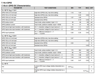
In the datasheet, there are conditions for the duration of the signal, but no conditions for the signal level.

At what voltage level will the signal trigger a reset?

Additionally, please let me know if there are any constraints regarding hysteresis and the rise time when resetting returns.

Regards.

  • Hello,

    I'm currently looking into this and will work to provide this information shortly.

    Regards,

    Andrew

  • I've confirmed that the RSTN pin will have the same characteristics as the GPIO. Please see table 7.19.4.1 of the data sheet for detailed information regarding voltage level thresholds for the RSTN pin.

    Regards,

    Andrew

  • Andrew, thank you for your response.

    It is very helpful.

    However, due to my poor understanding, could you please explain a bit more?

    Q1)Is my understanding correct that the section below means, 'Regardless of hysteresis, under 25℃ environmental conditions, it can be recognized as Low when the applied voltage is ×0.2V or less and High when the applied voltage is ×0.8V or more'?

    Q2)Does the result of Q1 change under temperature conditions? If it changes, could you provide data (such as graphs)?

    Q3)Is my understanding correct that the table below indicates that under the conditions of 3.8V & 25℃, the levels recognized as Low and High have a hysteresis of 0.40~0.47~0.54V? (I would like to confirm this because I didn't fully understand the condition of IH=1.)

    Q4)Could you please provide a little more explanation about the table below?

    Q5)Are there no constraints regarding the rise time and fall time of the reset signal mentioned in the initial post?

    I kindly ask for your support.

  • Hello,

    Q1) A low input (VIL) would be recognized when the applied voltage is 0.2*VDDS and a high (VIH) will be recognized when the applied voltage is 0.8*VDDS. So the thresholds are dependent on the supply voltage. If the device is operating with a supply voltage of 1.8VDC, then the low voltage threshold would be 0.2*1.8V = 0.36VDC. So if a voltage of 0.36VDC or lower was applied to the pin, then that would be recognized as a logic low. For a high the threshold would be 0.8*1.8V= 1.44VDC. So if a voltage of 1.44VDC or higher was applied to the pin, then that would be recognized as a logic high.

    Q2) I believe there will be some variation over temperature. I will have to reach out to another internal group to see if we have any data we can share.

    Q3) I'm sorry I wasn't clear on this in my initial response, for the RSTN pin there is no hysteresis. The voltage applied to RSTN must be below VIL to reset and above VIH to release reset. For GPIO, this spec in the table is stating that the hysteresis at a minimum can be as low as 0.4V, typically though it is 0.47V, and at a maximum can be 0.54V when the HYSTEN register is set to a 1 (Input Hysteresis IH=1). You can get more information about the input hysteresis register for the GPIO in section 18.5 of the TRM linked here.  But again these hysteresis specs do not apply to the RSTN pin.  

    Q4) This only applies to GPIO and not the RSTN pin but, this is stating that at 25C with VDDS= 3.8VDC, the transition from a logic 0 to a logic 1 can occur with a minimum voltage of 1.76V, but typically occurs at 1.98V, and can occur at a maximum of 2.27V. The transition from a logic 1 to a logic 0 can occur with a minimum voltage of 1.26V, but typically occurs at 1.52V, and can occur at a maximum of 1.79V. And again this applies when the GPIO HYSTEN register is set to 1 (Input Hysteresis IH=1).

    Q5) If you look at the LP-EM-CC2340R5 reference design linked here, you'll see that a 100kohm pull-up resistor and a 100nF capacitor tied to GND are connected to the reset line.  This is the recommended implementation of the device and provides the appropriate rise and fall time for the reset pin of the device. 

    Regards,

    Andrew

  • Hello.

    Thank you for your prompt response.

    Regarding Q2, please continue to verify the data.

    I understand very well from Q3 and Q4 that the RST pin does not have hysteresis.

    To ensure we are on the same page, please allow me to confirm.

    When I calculate based on the information you provided, it results in a discrepancy with the table values.

    Please let me know the formula that matches the table values when there is hysteresis (HYSTEN = 1).

    ex)3.8V×0.2+0.40V=1.23V

    I'm sorry to trouble you repeatedly, but I'd appreciate your cooperation.

    Regards.

  • Hello,

    The VIH and VIL formulas provide the voltage level required for consistent reliable interpretation of logic highs and lows.

    The low to high, high to low, and input hysteresis parameters detail specifics about voltage levels when hysteresis is enabled on a GPIO pin. For example with hysteresis enabled with Ta = 25C and VDDS = 3.8V, a GPIO can have an input voltage transition from 0 -> 1 in the range of 1.76V to 2.27V. Similarly a GPIO can have an input voltage transition from 1 -> 0 in the range of 1.26V to 1.79V. So if you have a device GPIO that has an input voltage transition from 0 -> 1 of 1.76V then the difference between this level and the input voltage transition from 1 -> 0 can be in the range of 0.4 to 0.54. Meaning that the input voltage transition from 1 -> 0 for this GPIO can range from 1.36V to 1.26V. This brings up another question of 1.76V - 0.54V = 1.22V, so why did I say the range is from 1.36V to 1.26V? That's because the minimum voltage level for the input voltage transition from 1->0 is 1.26V. I hope this clears up any confusion. 

    Regards,

    Andrew

  • Hello,

    I've confirmed that the VIH minimum (0.8*VDDS) and VIL maximum (0.2*VDDS) values in the datasheet are valid across the operating temperature range. 

    Regards,

    Andrew

  • Hi, Andrew.

    You have been very helpful.

    I will close this post.

    Thanks again.