This thread has been locked.

If you have a related question, please click the "Ask a related question" button in the top right corner. The newly created question will be automatically linked to this question.

CC2745R10-Q1: Schematic design review

Part Number: CC2745R10-Q1

Tool/software:

Dear Experts,

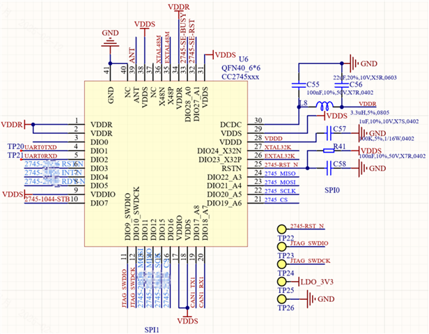
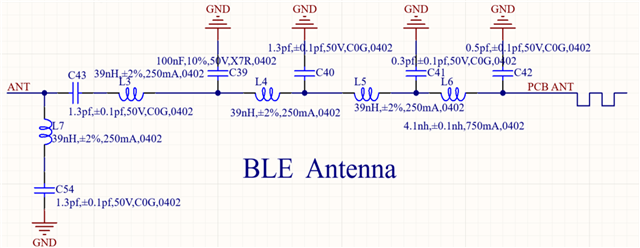
The following is the schematic diagram of CC2745.

Please help review whether the peripheral schematic design and ANT schematic design of CC2745 need to be optimized. Additionally, we have some questions regarding the design and hope to receive answers. Thank you very much
1. If CC2745 is used as a slave, which pins can be used as INT/WAKUP function pins
2. Is it necessary to reserve a reset circuit externally when using CC2745 as an MCU
3. For the convenience of subsequent debugging, which pins are recommended to reserve test points
  • Colin,

    1. All GPIO have  wakeup and interrupt capabilities.

    2. It is not necessary for the device to function but depending on the application requirements it may be useful. 

    3. The JTAG pins can be routed to a connector for debug purposes. VDDR and VDDS can also be useful test points as well as any other application specific IO that are deemed critical by the user. 

    As for the schematic review, please submit any design review requests at the following link:

    https://www.ti.com/tool/SIMPLELINK-2-4GHZ-DESIGN-REVIEWS

    Regards,

    Andrew
