This thread has been locked.

If you have a related question, please click the "Ask a related question" button in the top right corner. The newly created question will be automatically linked to this question.

CC2651R3SIPA: Voltage supply for high accuracy ADC

Part Number: CC2651R3SIPA

Tool/software:

We are developing an application that uses BLE and ADC using CC2651R3SIPA .
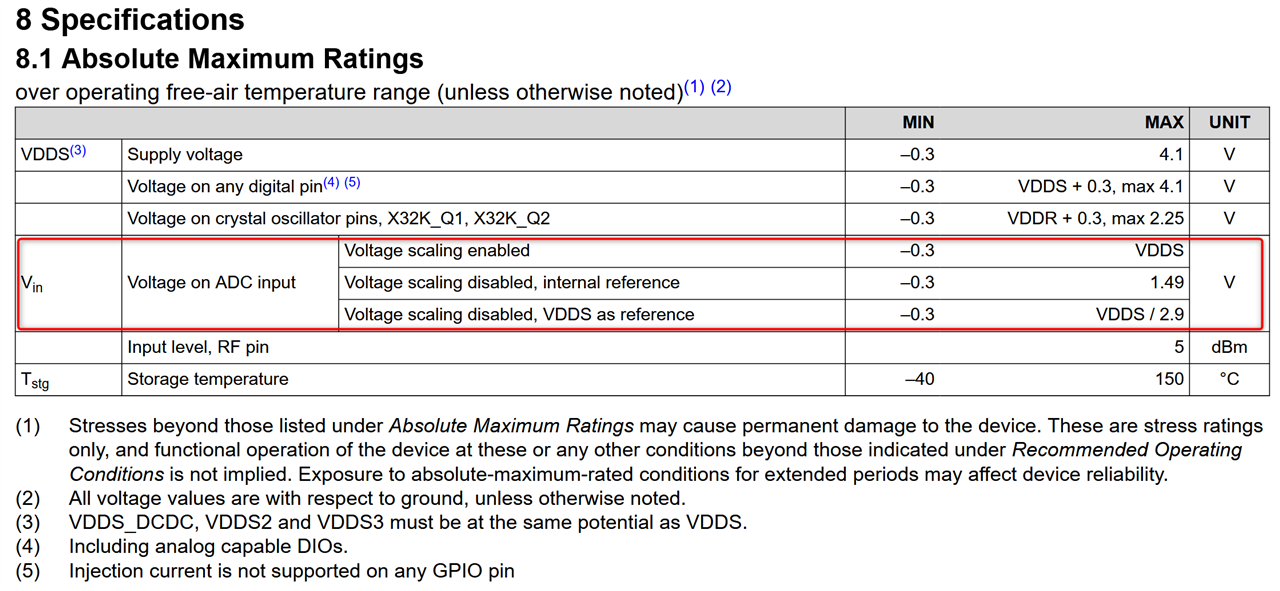
In the CC2651R3SIPA, the power supply pin for operation and the ADC reference voltage pin are integrated. We want to achieve an ADC accuracy of 0.5% or less. However, considering the supply current (around 100mA), there are no LDOs with 1% accuracy that meet this, and reference voltage ICs with 0.5% accuracy (with an output current of about 20mA) do not provide enough supply current for operation.

Do you have any suggestions on how to improve the ADC accuracy by increasing the ADC reference voltage accuracy?
Alternatively, are there any power supply ICs that can meet the required supply current and provide 0.5% or better accuracy?

  • Hi Toshio, 

    I am not entirely sure I understand your question. The internal ADC has a fixed reference voltage that is quite independent of the supply voltage and, when used with our drivers, uses the internal calibration and offset values to compensate any deviations on the device.

    One thread where this is mention is shown below. 

    https://e2e.ti.com/support/wireless-connectivity/bluetooth-group/bluetooth/f/bluetooth-forum/1173880/cc2652r7-adc-compensation 

    Also, depending on the configuration of scaling and reference source, it can achieve different degrees of effective number of bits (ENOB) from 9.8 to 11.3 bits. These precision figures can be helpful to perform additional calibration to your final product, including any compensation for the input signal chain it needed. 

    Hopefully this is what you were looking for but please let me know if there are any additional comments. 

    Regards,

    Rafael

  • Dear Rafael,

    Thank you very much for your excellent explanation. It helped us significantly deepen our understanding.

    We still have a few follow-up questions.
    As background, our system is operating under the following conditions:

    - VDDS = 2.5 V (±1%)
    - ADC input range = 0 to 2.5 V (since the "ADC Input Voltage Range" is specified as 0–VDDS)

    For the ADC configuration, we have selected:
    - Reference voltage = VDDS
    - Input voltage scaling = enabled

    Based on this, we would like to confirm the following points:

    Q1:
    We understand that the accuracy of the reference voltage (such as its offset and noise) has a direct impact on ADC precision.
    In terms of overall accuracy, which option would provide better performance: using VDDS or using the internal fixed reference voltage?

    Q2:
    When using the internal reference, we see that there are two available settings:
    - 4.3 V / input voltage scaling is enabled
    - 1.48 V /  input voltage scaling is disabled
    In these two cases, what is the corresponding ADC input full-scale voltage range?

    Q3:
    If we choose the 4.3 V internal reference with input scaling enabled, does it mean that the ADC's full-scale input range is 0–4.3 V, even though the actual maximum input voltage (due to VDDS limitation) is only up to 2.5 V?

    These may be basic questions, but your guidance would be greatly appreciated.
    We want to ensure proper understanding and safe operation of the device.

    Thank you very much in advance for your support.

    Best regards,

  • Hi,

    I would strongly recommend you to read section 19.4.2 of the Technical Reference Manual (TRM) which contains the detailed description of the ADC peripheral. 

    Q1: as you can imagine, the internal reference voltage has the best accuracy and precision. 

    Q2: the scaling will add some uncertainty to the ADC, as stated on the TRM section mentioned above and on the specifications shown in section 8.16 of the device datasheet. The input voltages are shown in section 8.1 of the device datasheet as well.  

    Q3: as you mentioned and is shown in the screenshot above, the maximum input voltage to the device is VDDS. 

    As an additional resource to better understand the ADC and its configuration settings, please check the ADC example projects in the URLs below, which are also present in our Simplelink SDK software

    https://dev.ti.com/tirex/explore/node?node=A__AMAR.2gMr4qn3LMqlm3p2Q__com.ti.SIMPLELINK_CC13XX_CC26XX_SDK__BSEc4rl__LATEST

    https://dev.ti.com/tirex/explore/node?node=A__APP-UMXOF906esqlKB4Lug__com.ti.SIMPLELINK_CC13XX_CC26XX_SDK__BSEc4rl__LATEST

    Hope this helps,

    Rafael

  • Hi, 
    Thank you for good advices.
    We'll check your suggestion and docs.

    From a PCB and hardware design standpoint, could you explain the factors that affect the ADC?
    For instance, under what conditions might its performance degrade—such as when the on-chip DC/DC converter is enabled?
    I’d also like to know the optimal conditions, settings, power supply and precautions for maximizing ADC accuracy.

    Regards.

  • Deard , and all

    Could you please answer the question I sent earlier?

  • Dear Rafael and TI teams,

    Could you please answer the question I sent earlier?

    Regards.

  • Hi Toshio,

    Please apologize for the delay in your reply. I was sidetracked by some escalations and missed your last post. 

    From a PCB and hardware design standpoint, could you explain the factors that affect the ADC?

    There are many factors that can affect the ADC performance, most of all related to noise that is coming from either the power supply, improper ground or even EMI. From a pure PCB / design standpoint, the proper decoupling of the device can help mitigate power supply issues. The routing of the ADC input can be shielded using guard traces or be forced to cross tracks on other layers in a perpendicular pattern to reduce coupling and crosstalk. EMI can be mitigated by using shielding on sensitive parts of the circuit, although this can become an expensive alternative and is typically used on systems with much higher ADC resolutions. 

    There are many references about this on the internet. A few are shown below:

    Page 68 of the Analog Engineer's Circuit Cookbook talks about PCB guard traces, among other details. 

    A general discussion about SAR ADCs (the type used in our devices) is shown in the following articles:

     SAR ADC PCB Layout: The reference path 

     Input considerations for SAR ADCs 

     Performance comparison between SAR ADC input types – Part 1    

    For instance, under what conditions might its performance degrade—such as when the on-chip DC/DC converter is enabled?

    While in theory the DC/DC converter can increase EMI, in our experience the reference design (Launchpad) does a good job in mitigating this

    I’d also like to know the optimal conditions, settings, power supply and precautions for maximizing ADC accuracy.

    I would check the performance specifications in sections 8.16.1 and 8.17.6 of the device datasheet. 

    Hope this helps,

    Rafael

  • Dear Desouza,

    Thank you very much for your help.
    We apologize for the late reply, but our concerns have now been resolved. We truly appreciate your support.

    Should we have any further questions, we will start a new thread.

    Best regard.